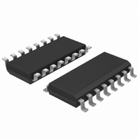
74HCT670D,653 NXP Semiconductors, 74HCT670D,653 Datasheet - Page 2

74HCT670D,653
Manufacturer Part Number
74HCT670D,653
Description
IC 4X4 REGISTER FILE 3ST 16SOIC
Manufacturer
NXP Semiconductors
Series
74HCTr
Datasheet
1.74HCT670DB112.pdf
(9 pages)
Specifications of 74HCT670D,653
Logic Type
Register, Bidirectional
Package / Case
16-SOIC (3.9mm Width)
Output Type
Standard
Number Of Elements
1
Number Of Bits Per Element
4
Function
Universal
Voltage - Supply
4.5 V ~ 5.5 V
Operating Temperature
-40°C ~ 125°C
Mounting Type
Surface Mount
Logic Family
HCT
Number Of Circuits
1
Propagation Delay Time
50 ns
High Level Output Current
- 6 mA
Low Level Output Current
6 mA
Supply Voltage (max)
5.5 V
Maximum Operating Temperature
+ 125 C
Minimum Operating Temperature
- 40 C
Mounting Style
SMD/SMT
Supply Voltage (min)
4.5 V
Logical Function
Register File
Number Of Elements
1
Number Of Bits
4
Number Of Inputs
4
Number Of Outputs
4
Operating Supply Voltage (typ)
5V
Operating Supply Voltage (max)
5.5V
Operating Supply Voltage (min)
4.5V
Polarity
Non-Inverting
Technology
CMOS
Mounting
Surface Mount
Pin Count
16
Operating Temp Range
-40C to 125C
Operating Temperature Classification
Automotive
Quiescent Current
8uA
Lead Free Status / RoHS Status
Lead free / RoHS Compliant
Lead Free Status / RoHS Status
Lead free / RoHS Compliant, Lead free / RoHS Compliant
Other names
74HCT670D-T
74HCT670D-T
933715410653
74HCT670D-T
933715410653
Philips Semiconductors
FEATURES
GENERAL DESCRIPTION
The 74HC/HCT670 are high-speed Si-gate CMOS devices
and are pin compatible with low power Schottky TTL
(LSTTL). They are specified in compliance with JEDEC
standard no. 7A.
The 74HC/HCT670 are 16-bit 3-state register files
organized as 4 words of 4 bits each. Separated read and
write address inputs (R
inputs (RE and WE) are available, permitting simultaneous
writing into one word location and reading from another
location. The 4-bit word to be stored is presented to four
data inputs (D
QUICK REFERENCE DATA
GND = 0 V; T
Notes
1. C
2. For HC the condition is V
ORDERING INFORMATION
See
December 1990
SYMBOL PARAMETER
t
C
C
PHL
Simultaneous and independent read and write
operations
Expandable to almost any word size and bit length
Output capability: bus driver
I
4 x 4 register file; 3-state
I
PD
CC
f
f
C
V
for HCT the condition is V
i
o
“74HC/HCT/HCU/HCMOS Logic Package Information”
/ t
CC
PD
L
category: MSI
= output frequency in MHz
= input frequency in MHz
(C
PLH
= output load capacitance in pF
P
is used to determine the dynamic power dissipation (P
= supply voltage in V
L
D
= C
V
propagation delay D
input capacitance
power dissipation capacitance per package
amb
CC
0
PD
to D
2
= 25 C; t
V
3
f
o
). The W
CC
) = sum of outputs
A
2
, R
f
r
B
i
= t
and W
A
I
I
f
= GND to V
and W
= GND to V
= 6 ns
(C
n
to Q
L
A
, W
B
V
n
inputs determine
CC
B
) and enable
2
CC
CC
;
f
1.5 V
o
)
where:
2
.
CONDITIONS
C
notes 1 and 2
the location of the stored word. When the WE input is
LOW, the data is entered into the addressed location. The
addressed location remains transparent to the data while
the WE input is LOW. Data supplied at the inputs will be
read out in true (non-inverting) form from the 3-state
outputs (Q
WE is HIGH.
Direct acquisition of data stored in any of the four registers
is made possible by individual read address inputs
(R
outputs when the RE is LOW. Data outputs are in the high
impedance OFF-state when RE is HIGH. This permits
outputs to be tied together to increase the word capacity to
very large numbers.
Design of the read enable signals for the stacked devices
must ensure that there is no overlap in the LOW levels
which would cause more than one output to be active at
the same time. Parallel expansion to generate n-bit words
is accomplished by driving the enable and address inputs
of each device in parallel.
L
D
= 15 pF; V
A
in W):
and R
B
0
). The addressed word appears at the four
to Q
CC
= 5 V
3
). D
n
and W
23
3.5
122
n
inputs are inhibited when
HC
74HC/HCT670
TYPICAL
Product specification
23
3.5
124
HCT
ns
pF
pF
UNIT


