74HCT670D,653 NXP Semiconductors, 74HCT670D,653 Datasheet - Page 3
74HCT670D,653
Manufacturer Part Number
74HCT670D,653
Description
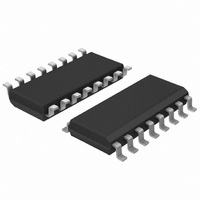
IC 4X4 REGISTER FILE 3ST 16SOIC
Manufacturer
NXP Semiconductors
Series
74HCTr
Datasheet
1.74HCT670DB112.pdf
(9 pages)
Specifications of 74HCT670D,653
Logic Type
Register, Bidirectional
Package / Case
16-SOIC (3.9mm Width)
Output Type
Standard
Number Of Elements
1
Number Of Bits Per Element
4
Function
Universal
Voltage - Supply
4.5 V ~ 5.5 V
Operating Temperature
-40°C ~ 125°C
Mounting Type
Surface Mount
Logic Family
HCT
Number Of Circuits
1
Propagation Delay Time
50 ns
High Level Output Current
- 6 mA
Low Level Output Current
6 mA
Supply Voltage (max)
5.5 V
Maximum Operating Temperature
+ 125 C
Minimum Operating Temperature
- 40 C
Mounting Style
SMD/SMT
Supply Voltage (min)
4.5 V
Logical Function
Register File
Number Of Elements
1
Number Of Bits
4
Number Of Inputs
4
Number Of Outputs
4
Operating Supply Voltage (typ)
5V
Operating Supply Voltage (max)
5.5V
Operating Supply Voltage (min)
4.5V
Polarity
Non-Inverting
Technology
CMOS
Mounting
Surface Mount
Pin Count
16
Operating Temp Range
-40C to 125C
Operating Temperature Classification
Automotive
Quiescent Current
8uA
Lead Free Status / RoHS Status
Lead free / RoHS Compliant
Lead Free Status / RoHS Status
Lead free / RoHS Compliant, Lead free / RoHS Compliant
Other names
74HCT670D-T
74HCT670D-T
933715410653
74HCT670D-T
933715410653


Philips Semiconductors
PIN DESCRIPTION
WRITE MODE SELECT TABLE
Note
1. The write address (W
December 1990
PIN NO.
5, 4
8
10, 9, 7, 6
11
12
14, 13
15, 1, 2, 3
16
OPERATING
MODE
write data
data latched
4 x 4 register file; 3-state
“internal latches” must be stable while WE is
LOW for conventional operation.
Fig.2 Logic symbol.
SYMBOL
R
GND
Q
RE
WE
W
D
V
A
0
CC
0
A
, R
, W
to D
to Q
L
L
H
WE
B
INPUTS
B
3
3
L
H
X
A
D
and W
n
NAME AND FUNCTION
read address inputs
ground (0 V)
data outputs
3-state output read enable input (active LOW)
write enable input (active LOW)
write address inputs
data inputs
positive supply voltage
INTERNAL
LATCHES
L
H
no change
B
) to the
(1)
Fig.3 IEC logic symbol.
READ MODE SELECT TABLE
Notes
1. The selection of the “internal latches” by read address
OPERATING
MODE
read
disabled
(R
H = HIGH voltage level
L = LOW voltage level
X = don’t care
Z = high impedance OFF-state
3
A
and R
B
) are not constrained by WE or RE operation.
RE
H
L
L
INTERNAL LATCHES
INPUTS
Fig.4 Functional diagram.
Fig.1 Pin configuration.
H
X
L
74HC/HCT670
Product specification
(1)
OUTPUT
Q
H
L
Z
n
Related parts for 74HCT670D,653
Image
Part Number
Description
Manufacturer
Datasheet
Request
R

Part Number:
Description:
4 X 4 Register File; 3-state
Manufacturer:
NXP Semiconductors
Datasheet:

Part Number:
Description:
IC BUFF/DVR TRI-ST DUAL 20DIP
Manufacturer:
Fairchild Semiconductor
Datasheet:

Part Number:
Description:
IC BUS TRANSCVR 3-ST 8BIT 20DIP
Manufacturer:
ON Semiconductor
Datasheet:

Part Number:
Description:
IC TRANSCEIVER 3-ST 8BIT 20SOIC
Manufacturer:
Fairchild Semiconductor
Datasheet:

Part Number:
Description:
IC BUFFER NONINV QUAD 3ST 14SOIC
Manufacturer:
ON Semiconductor
Datasheet:
Part Number:
Description:
IC BUFFER NONINV QUAD 3ST 14SOIC
Manufacturer:
ON Semiconductor
Datasheet:

Part Number:
Description:
IC BUS TRANSCVR 3-ST 8BIT 20SOIC
Manufacturer:
ON Semiconductor
Datasheet:

Part Number:
Description:
IC BUFF/DVR TRI-ST 8BIT 20SOIC
Manufacturer:
ON Semiconductor
Datasheet:

Part Number:
Description:
IC FLIP FLOP OCT D 3ST 20TSSOP
Manufacturer:
Fairchild Semiconductor
Datasheet:

Part Number:
Description:
IC FLIP FLOP OCTAL D 20-DIP
Manufacturer:
STMicroelectronics
Datasheet:

Part Number:
Description:
IC FLIP FLOP DUAL D-TYPE 14-SOIC
Manufacturer:
Fairchild Semiconductor
Datasheet:
Part Number:
Description:
IC FLIP FLOP OCTAL D 20-SOIC
Manufacturer:
Fairchild Semiconductor
Datasheet:

Part Number:
Description:
IC FLIP FLOP OCT D 3ST 20-SOIC
Manufacturer:
ON Semiconductor
Datasheet:

Part Number:
Description:
IC INVERT HEX SCHM TRIG 14-SOIC
Manufacturer:
ON Semiconductor
Datasheet:

Part Number:
Description:
IC INVERTER HEX LSTTL IN 14TSSOP
Manufacturer:
ON Semiconductor
Datasheet: