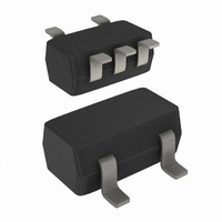
74CBTLV1G125GW,125 NXP Semiconductors, 74CBTLV1G125GW,125 Datasheet - Page 9

74CBTLV1G125GW,125
Manufacturer Part Number
74CBTLV1G125GW,125
Description
IC SINGLE BUS SWITCH 5-TSSOP
Manufacturer
NXP Semiconductors
Series
74CBTLVr
Type
FET Bus Switchr
Datasheet
1.74CBTLV1G125GV125.pdf
(21 pages)
Specifications of 74CBTLV1G125GW,125
Package / Case
SC-70-5, SC-88A, SOT-323-5, SOT-353, 5-TSSOP
Circuit
1 x 1:1
Independent Circuits
1
Voltage Supply Source
Single Supply
Voltage - Supply
2.3 V ~ 3.6 V
Operating Temperature
-40°C ~ 125°C
Mounting Type
Surface Mount
Logic Family
CBTLV
On Resistance (max)
11 Ohms
Propagation Delay Time
0.16 ns
Maximum Operating Temperature
+ 125 C
Minimum Operating Temperature
- 40 C
Function
Bus Switch
High Level Output Current
- 128 mA
Low Level Output Current
128 mA
Mounting Style
SMD/SMT
Operating Supply Voltage
2.5 V, 3.3 V
Organization
1 x 1:1
Supply Voltage (max)
3.6 V
Supply Voltage (min)
2.3 V
Logic Type
CMOS
Number Of Circuits
1
Lead Free Status / RoHS Status
Lead free / RoHS Compliant
Current - Output High, Low
-
Lead Free Status / Rohs Status
Lead free / RoHS Compliant
Other names
568-4833-2
74CBTLV1G125GW,125
74CBTLV1G125GW-G
74CBTLV1G125GW-G
935280319125
74CBTLV1G125GW,125
74CBTLV1G125GW-G
74CBTLV1G125GW-G
935280319125
NXP Semiconductors
11. Dynamic characteristics
Table 9.
GND = 0 V; see
[1]
[2]
[3]
[4]
[5]
12. Waveforms
Table 10.
74CBTLV1G125
Product data sheet
Symbol Parameter
t
t
t
Supply voltage
V
2.3 V to 3.6 V
pd
en
dis
Fig 11. The data input (A or B) to output (B or A) propagation delays
CC
All typical values are measured at T
The propagation delay is the calculated RC time constant of the maximum on-state resistance of the switch and the load capacitance,
when driven by an ideal voltage source (zero output impedance).
t
t
t
pd
en
dis
is the same as t
is the same as t
is the same as t
propagation delay A to B or B to A;
enable time
disable time
Measurement points are given in
Logic levels: V
Dynamic characteristics
Measurement points
Figure
PLH
PZH
PHZ
13.
OL
and t
and t
and t
and V
PHL
PZL
PLZ
Output
V
0.5 × V
Conditions
see
OE to A or B; see
R
OE to A or B; see
R
OH
M
L
L
.
.
.
V
V
V
V
V
V
= 500 Ω
= 500 Ω
are typical output voltage drop that occur with the output load.
CC
CC
CC
CC
CC
CC
A or B
B or A
output
Figure
input
amb
= 2.3 V to 2.7 V
= 3.0 V to 3.6 V
= 2.3 V to 2.7 V
= 3.0 V to 3.6 V
= 2.3 V to 2.7 V
= 3.0 V to 3.6 V
CC
GND
V
V
= 25 °C and at nominal V
OH
Table
OL
V
11; R
I
All information provided in this document is subject to legal disclaimers.
10.
L
Figure
Figure
= ∞ Ω
Rev. 2 — 29 July 2010
V
Inputs
V
0.5 × V
M
12;
12;
M
t
PLH
CC
[2][3]
CC
[4]
[5]
V
.
M
V
Min
M
1.0
1.0
1.0
1.0
-
-
−40 °C to +85 °C
t
PHL
Typ
V
V
V
0.16
2.50
2.05
2.80
3.40
M
I
CC
-
[1]
001aad719
Max
0.21
0.25
4.00
4.00
5.00
4.10
74CBTLV1G125
−40 °C to +125 °C
Min
1.0
1.0
1.0
1.0
-
-
t
≤ 2.0 ns
r
Single bus switch
= t
© NXP B.V. 2010. All rights reserved.
f
Max
0.32
0.39
5.00
5.00
6.30
5.40
9 of 21
Unit
ns
ns
ns
ns
ns
ns


