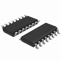
CBT3253AD,112 NXP Semiconductors, CBT3253AD,112 Datasheet - Page 4

CBT3253AD,112
Manufacturer Part Number
CBT3253AD,112
Description
IC 1-OF-4 FET MUX/DEMUX 16SOIC
Manufacturer
NXP Semiconductors
Series
74CBTr
Type
FET Multiplexer/Demuxr
Datasheet
1.CBT3253APW118.pdf
(17 pages)
Specifications of CBT3253AD,112
Package / Case
16-SOIC (3.9mm Width)
Circuit
2 x 1:4
Independent Circuits
1
Current - Output High, Low
15mA, 64mA
Voltage Supply Source
Single Supply
Voltage - Supply
4.5 V ~ 5.5 V
Operating Temperature
-40°C ~ 85°C
Mounting Type
Surface Mount
Product
Multiplexer
Logic Family
CBT
Number Of Lines (input / Output)
8.0 / 2.0
Propagation Delay Time
0.25 ns
Supply Voltage (max)
5.5 V
Supply Voltage (min)
4.5 V
Maximum Operating Temperature
+ 85 C
Minimum Operating Temperature
- 40 C
Mounting Style
SMD/SMT
Number Of Input Lines
8.0
Number Of Output Lines
2.0
Number Of Bits
8
Number Of Elements
1
Technology
CMOS
On Resistance
10Ohm
Package Type
SO
Operating Temp Range
-40C to 85C
Operating Temperature Classification
Industrial
Operating Supply Voltage (min)
4.5V
Operating Supply Voltage (typ)
5V
Operating Supply Voltage (max)
5.5V
Quiescent Current
3uA
Pin Count
16
Mounting
Surface Mount
Lead Free Status / RoHS Status
Lead free / RoHS Compliant
Lead Free Status / RoHS Status
Lead free / RoHS Compliant, Lead free / RoHS Compliant
Other names
568-3055-5
935275884112
CBT3253AD
935275884112
CBT3253AD
NXP Semiconductors
6. Functional description
7. Limiting values
8. Recommended operating conditions
CBT3253A_2
Product data sheet
6.1 Function selection
Refer to
Table 3.
H = HIGH state; L = LOW state; X = Don’t Care
Table 4.
In accordance with the Absolute Maximum Rating System (IEC 60134).
[1]
Table 5.
All unused control inputs of the device must be held at V
operation.
Inputs
1OE
X
H
L
L
L
L
Symbol
V
V
I
I
T
Symbol
V
V
V
T
CCC
IK
stg
amb
CC
I
CC
IH
IL
The input and output negative voltage ratings may be exceeded if the input and output clamp current ratings
are observed.
2OE
H
X
L
L
L
L
Figure 1 “Logic diagram of CBT3253A (positive logic)”
Parameter
supply voltage
input voltage
continuous current through
each V
input clamping current
storage temperature
Parameter
supply voltage
HIGH-level input voltage
LOW-level input voltage
ambient temperature
Function selection
Limiting values
Operating conditions
S1
X
X
L
L
H
H
CC
or GND pin
Rev. 02 — 8 February 2007
S0
X
X
L
H
L
H
Function
disconnect 1A and 2A
disconnect 1A and 2A
1A to 1B1 and 2A to 2B1
1A to 1B2 and 2A to 2B2
1A to 1B3 and 2A to 2B3
1A to 1B4 and 2A to 2B4
Conditions
operating in free air
Conditions
V
I
< 0 V
Dual 1-of-4 FET multiplexer/demultiplexer
CC
or GND to ensure proper device
Min
4.5
2
-
40
Min
-
-
0.5
0.5
65
[1]
Typ
-
-
-
-
CBT3253A
Max
+7.0
+7.0
128
+150
© NXP B.V. 2007. All rights reserved.
50
Max
5.5
-
0.8
+85
Unit
V
V
mA
mA
C
Unit
V
V
V
4 of 17
C


