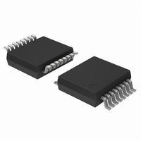
PCA8550DB,118 NXP Semiconductors, PCA8550DB,118 Datasheet - Page 3

PCA8550DB,118
Manufacturer Part Number
PCA8550DB,118
Description
IC I2C EEPROM DIP SWITCH 16SSOP
Manufacturer
NXP Semiconductors
Type
Multiplexerr
Datasheet
1.PCA8550PW118.pdf
(12 pages)
Specifications of PCA8550DB,118
Circuit
1 x 4:4
Independent Circuits
1
Current - Output High, Low
2mA, 2mA
Voltage Supply Source
Single Supply
Voltage - Supply
3 V ~ 3.6 V
Operating Temperature
0°C ~ 70°C
Mounting Type
Surface Mount
Package / Case
16-SSOP
Lead Free Status / RoHS Status
Lead free / RoHS Compliant
Other names
935261458118
PCA8550DB-T
PCA8550DB-T
PCA8550DB-T
PCA8550DB-T
Philips Semiconductors
PIN DESCRIPTION
FUNCTION TABLE
Table 1. Function table
NOTE
1. Latched NON_MIXED_OUT state will be the value present on
2003 Jun 27
NUMBER
OVERRIDE
4-bit multiplexed/1-bit latched 5-bit
I
the NON_MUXED_OUT output at the time of the MUX_SELECT
input transitioned from a logic 0 to a logic 1 state.
2
PIN
10
12
13
14
15
16
11
1
2
3
4
5
6
7
8
9
C EEPROM DIP switch
_N
0
0
1
1
NON_MUXED_OUT
MUX_SELECT
MUX_SELECT
OVERRIDE_N
MUX_OUT D
MUX_OUT C
MUX_OUT B
MUX_OUT A
MUX_IN A
MUX_IN B
MUX_IN C
MUX_IN D
SYMBOL
I
I
2
2
C SCL
C SDA
GND
V
WP
0
1
0
1
CC
MUX_OUT
OUTPUTS
From non-
MUX_IN
MUX_IN
register
volatile
All 0’s
inputs
inputs
I
Bi-directional I
Forces all outputs to logic 0
External inputs to multiplexer
Common ground voltage rail
2.5 V multiplexed output
Selects MUX_IN inputs or
register contents for
MUX_OUT outputs
TTL-level output from
non-volatile memory
Non-volatile register
write-protect
Positive voltage rail
2
C-bus clock
FUNCTION
NON_MUXED_OUT
NON_MUXED_OUT
From non-volatile
From non-volatile
2
C-bus data
OUTPUT
Latched
register
register
All 0’s
1
3
I
Communicating with this device is initiated by sending a valid
address on the I
unique 7-bit value followed by a 1-bit read/write value which
determines the direction of the data transfer.
Following the address and acknowledge bit are 8 data bits which,
depending on the read/write bit in the address, will read data from or
write data to the non-volatile register. Data will be written to the
register if the read/write bit is logic 0 and the WP input is logic 0.
Data will be read from the register if the bit is logic 1. The three
high-order bits (see FIgure 3) are logic 0. The next bit is data which
is non-multiplexed. The low four bits are the data which will be
multiplexed. A write with any of the first three bits non-zero will be
aborted.
NOTE:
1. To ensure data integrity, the non-volatile register must be
POWER-ON RESET (POR)
When power is applied to V
PCA8550 in a reset state until V
the reset condition is released and the PCA8550 volatile registers
and I
The MUX_OUT and NON_MUXED_OUT pin values depend on:
2
C INTERFACE
- the OVERRIDE_N and MUX_SELECT logic levels
- the previously stored values in the EEPROM register/current
internally write protected when V
down or V
operating levels.
MSB
MUX_IN pin values as shown in Table 1.
2
0
C state machine will initialize to their default states.
MSB
1
CC
0
2
0
to the component is dropped below normal
C-bus. The address format (see FIgure 2) is a fixed
Figure 2. I
Figure 3. I
0
0
MUXED
NON-
DATA
CC
1
, an internal power-on reset holds the
2
C Address Byte
CC
2
C Data Byte
1
DATA D
has reached V
MUX
CC
to the I
1
DATA C
MUX
2
0
C-bus is powered
PCA8550
DATA B
POR
MUX
R/W
LSB
. At that point,
Product data
DATA A
MUX
LSB


