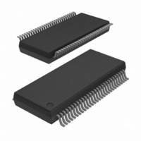
CBT16212DL,512 NXP Semiconductors, CBT16212DL,512 Datasheet - Page 5

CBT16212DL,512
Manufacturer Part Number
CBT16212DL,512
Description
IC BUS SWITCH 24BIT 56SSOP
Manufacturer
NXP Semiconductors
Series
74CBTr
Type
Bus Switchr
Datasheet
1.CBT16212DGG118.pdf
(12 pages)
Specifications of CBT16212DL,512
Circuit
12 x 2:2
Independent Circuits
1
Current - Output High, Low
15mA, 64mA
Voltage Supply Source
Single Supply
Voltage - Supply
4 V ~ 5.5 V
Operating Temperature
-40°C ~ 85°C
Mounting Type
Surface Mount
Package / Case
56-SSOP
Lead Free Status / RoHS Status
Lead free / RoHS Compliant
Other names
935270391512
CBT16212DL
CBT16212DL
CBT16212DL
CBT16212DL
NXP Semiconductors
9. Static characteristics
Table 6.
T
[1]
[2]
[3]
10. Dynamic characteristics
Table 7.
T
[1]
[2]
[3]
[4]
CBT16212_2
Product data sheet
Symbol
V
I
I
C
C
R
Symbol
t
t
t
I
CC
pd
en
dis
amb
amb
I
IK
I
io(off)
ON
CC
All typical values are measured at T
This is the increase in supply current for each input that is at the specified TTL voltage level rather than V
Measured by the voltage drop between the A and the B terminals at the indicated current through the switch. ON resistance is
determined by the lowest voltage of the two (A or B) terminals.
This parameter is warranted but not production tested. The propagation delay is based on the RC time constant of the typical
ON resistance of the switch and a load capacitance of 50 pF, when driven by an ideal voltage source (zero output impedance).
t
t
t
pd
en
dis
= 40 C to +85 C.
= 40 C to +85 C; V
is the same as t
is the same as t
is the same as t
Parameter
input clamping voltage
input leakage current
supply current
additional supply current
input capacitance
off-state input/output capacitance V
ON resistance
Parameter
propagation delay
enable time
disable time
Static characteristics
Dynamic characteristics
PLH
PZL
PLZ
and t
and t
and t
CC
PZH
PHL
PHZ
= 4.5 V to 5.5 V; for test circuit see
.
.
.
amb
= 25 C.
Conditions
V
V
V
V
V
per port select input pin; V
one input at 3.4 V, other inputs at V
or GND
port select input pins; V
V
V
V
Conditions
input A or B to output B or A; see
port select input to output A or B;
port select input to output A or B;
CC
CC
CC
CC
I
CC
O
CC
CC
Rev. 02 — 3 November 2008
V
V
V
V
= V
= 3 V or 0 V; V
I
I
I
I
= 4.5 V; I
= 0 V; V
= 5.5 V; V
= 5.5 V; I
= 5.0 V;
= 4.0 V
= 4.5 V
= 2.4 V; I
= 0 V; I
= 0 V; I
= 2.4 V; I
CC
or GND
I
I
I
= 64 mA
= 30 mA
24-bit bus exchange switch with 12-bit output enables
I
O
= 5.5 V
I
I
I
= 18 mA
= 15 mA
= 15 mA
= V
= 0 A;
CC
Figure
CC
= 0 V
or GND
I
= 3 V or 0 V;
6.
CC
= 5.5 V;
Figure 4
Figure 5
Figure 5
CC
[2]
[3]
[3]
Min
-
-
-
-
-
-
-
-
-
-
-
[1][2]
[3]
[4]
CC
Typ
11.5
CBT16212
Min
or GND.
4.7
2.4
2.4
4
4
6
-
-
-
-
-
-
-
[1]
© NXP B.V. 2008. All rights reserved.
Max
Max
0.25
2.5
8.0
8.0
10
21
12
1.2
3
7
7
-
-
1
Unit
V
mA
pF
pF
Unit
ns
ns
ns
A
A
A
5 of 12


