CBTD16210DGG,512 NXP Semiconductors, CBTD16210DGG,512 Datasheet - Page 2
CBTD16210DGG,512
Manufacturer Part Number
CBTD16210DGG,512
Description
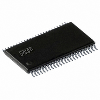
IC BUS SWITCH 20BIT 48-TSSOP
Manufacturer
NXP Semiconductors
Series
74CBTDr
Type
Bus Switchr
Datasheet
1.CBTD16210DGG518.pdf
(10 pages)
Specifications of CBTD16210DGG,512
Circuit
10 x 1:1
Independent Circuits
2
Voltage Supply Source
Single Supply
Voltage - Supply
4.5 V ~ 5.5 V
Operating Temperature
-40°C ~ 85°C
Mounting Type
Surface Mount
Package / Case
48-TSSOP
Lead Free Status / RoHS Status
Lead free / RoHS Compliant
Current - Output High, Low
-
Other names
935268484512
CBTD16210DG
CBTD16210DG
CBTD1621ODG
CBTD1621ODG
CBTD16210DG
CBTD16210DG
CBTD1621ODG
CBTD1621ODG


Philips Semiconductors
FEATURES
QUICK REFERENCE DATA
ORDERING INFORMATION
LOGIC SYMBOL
48-Pin Plastic SSOP Type III
48-Pin Plastic TSSOP Type II
2000 Oct 12
5 switch connection between two ports
TTL compatible control input levels
Designed to be used in 5.5 V to 3.3 V level shifting applications
Package options include shrink small outline (SSOP) and thin
shrink small outline (TSSOP)
20-bit level shifting bus switch
with 10-bit output enables
SYMBOL
C
t
t
I
C
CCZ
PLH
PHL
OUT
IN
1A10
2A10
1OE
2OE
1A1
2A1
PACKAGES
12
88
13
24
47
Propagation delay
An to Yn
Input capacitance
Output capacitance
Total supply current
2
PARAMETER
46
36
35
25
SA00545
1B1
1B10
2B1
2B10
TEMPERATURE RANGE
–40 C to +85 C
–40 C to +85 C
C
V
Outputs disabled; V
Outputs disabled; V
I
L
= 0V or V
= 50pF; V
CC
2
CC
T
amb
= 5V
DESCRIPTION
The CBTD16210 provides 20 bits of high-speed TTL-compatible bus
switching. The low on-state resistance of the switch allows
connections to be made with minimal propagation delay.
A diode to V
between 5 V inputs and 3.3 V outputs.
The device is organized as a dual 10-bit bus switch with separate
output-enable (OE) inputs. It can be used as two 10-bit bus switches
or as one 20-bit bus switch. When OE is low, the associated 10-bit
bus switch is on, and port A is connected to port B. When OE is
high, the switch is open, and a high-impedance state exists between
the ports.
The CBTD16210 is characterized for operation from –40 C to
+85 C.
FUNCTION TABLE
H = High voltage level
L = Low voltage level
Z = High impedance “off ” state
CONDITIONS
= 25 C; GND = 0V
CC
O
= 0V or V
1OE
= 5.5V
H
H
L
L
CC
INPUTS
CBTD16210 DGG
CBTD16210 DL
ORDER CODE
CC
is integrated in the circuit to allow for level shifting
2OE
H
H
L
L
1A = 1B
1A = 1B
1A, 1B
TYPICAL
Z
Z
0.25
CBTD16210
4.3
6.9
4.0
OUTPUTS
Product specification
DWG NUMBER
SOT370-1
SOT362-1
853-2221 24787
2A = 2B
2A = 2B
2A, 2B
Z
Z
UNIT
pF
pF
ns
A
Related parts for CBTD16210DGG,512
Image
Part Number
Description
Manufacturer
Datasheet
Request
R

Part Number:
Description:
Manufacturer:
NXP Semiconductors
Datasheet:
Part Number:
Description:
NXP Semiconductors designed the LPC2420/2460 microcontroller around a 16-bit/32-bitARM7TDMI-S CPU core with real-time debug interfaces that include both JTAG andembedded trace
Manufacturer:
NXP Semiconductors
Datasheet:

Part Number:
Description:
NXP Semiconductors designed the LPC2458 microcontroller around a 16-bit/32-bitARM7TDMI-S CPU core with real-time debug interfaces that include both JTAG andembedded trace
Manufacturer:
NXP Semiconductors
Datasheet:
Part Number:
Description:
NXP Semiconductors designed the LPC2468 microcontroller around a 16-bit/32-bitARM7TDMI-S CPU core with real-time debug interfaces that include both JTAG andembedded trace
Manufacturer:
NXP Semiconductors
Datasheet:
Part Number:
Description:
NXP Semiconductors designed the LPC2470 microcontroller, powered by theARM7TDMI-S core, to be a highly integrated microcontroller for a wide range ofapplications that require advanced communications and high quality graphic displays
Manufacturer:
NXP Semiconductors
Datasheet:
Part Number:
Description:
NXP Semiconductors designed the LPC2478 microcontroller, powered by theARM7TDMI-S core, to be a highly integrated microcontroller for a wide range ofapplications that require advanced communications and high quality graphic displays
Manufacturer:
NXP Semiconductors
Datasheet:
Part Number:
Description:
The Philips Semiconductors XA (eXtended Architecture) family of 16-bit single-chip microcontrollers is powerful enough to easily handle the requirements of high performance embedded applications, yet inexpensive enough to compete in the market for hi
Manufacturer:
NXP Semiconductors
Datasheet:
Part Number:
Description:
The XA-S3 device is a member of Philips Semiconductors? XA(eXtended Architecture) family of high performance 16-bitsingle-chip microcontrollers
Manufacturer:
NXP Semiconductors
Datasheet:

Part Number:
Description:
The NXP BlueStreak LH75401/LH75411 family consists of two low-cost 16/32-bit System-on-Chip (SoC) devices
Manufacturer:
NXP Semiconductors
Datasheet:
Part Number:
Description:
The NXP LPC3130/3131 combine an 180 MHz ARM926EJ-S CPU core, high-speed USB2
Manufacturer:
NXP Semiconductors
Datasheet:
Part Number:
Description:
The NXP LPC3141 combine a 270 MHz ARM926EJ-S CPU core, High-speed USB 2
Manufacturer:
NXP Semiconductors
Part Number:
Description:
The NXP LPC3143 combine a 270 MHz ARM926EJ-S CPU core, High-speed USB 2
Manufacturer:
NXP Semiconductors

Part Number:
Description:
The NXP LPC3152 combines an 180 MHz ARM926EJ-S CPU core, High-speed USB 2
Manufacturer:
NXP Semiconductors
Part Number:
Description:
The NXP LPC3154 combines an 180 MHz ARM926EJ-S CPU core, High-speed USB 2
Manufacturer:
NXP Semiconductors