IDT728981J IDT, Integrated Device Technology Inc, IDT728981J Datasheet
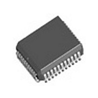
IC DGTL SW 256X256 44-PLCC

IDT728981J

Manufacturer Part Number
IDT728981J
Description
IC DGTL SW 256X256 44-PLCC
Manufacturer
IDT, Integrated Device Technology Inc
Series
7200r
Type
Multiplexerr
Datasheet

Specifications of IDT728981J

Circuit
1 x 4:4
Independent Circuits
1
Voltage Supply Source
Single Supply
Voltage - Supply
4.75 V ~ 5.25 V
Operating Temperature
-40°C ~ 85°C
Mounting Type
Surface Mount
Package / Case
44-PLCC
Lead Free Status / RoHS Status
Contains lead / RoHS non-compliant
Current - Output High, Low
-
Lead Free Status / RoHS Status
Not Compliant, Contains lead / RoHS non-compliant
Other names
728981J

Available stocks

Company
Part Number
Manufacturer
Quantity
Price
Part Number:
IDT728981J
Manufacturer:
NS
Quantity:
36
Part Number:
IDT728981J
Manufacturer:
IDT, Integrated Device Technology Inc
Quantity:
10 000
Part Number:
IDT728981J8
Manufacturer:
IDT, Integrated Device Technology Inc
Quantity:
10 000
Part Number:
IDT728981JG
Manufacturer:
IDT, Integrated Device Technology Inc
Quantity:
10 000
Part Number:
IDT728981JG8
Manufacturer:
IDT, Integrated Device Technology Inc
Quantity:
10 000
microprocessor. The IDT728981 can handle as many as 128, 64 Kbit/s input
and output channels. Those 128 channels are divided into 4 serial inputs and
RX0
RX1
RX2
RX3
2001 Integrated Device Technology, Inc.
The IDT728981 is a ST-BUS
128 x 128 channel non-blocking switch
Serial Telecom Bus Compatible (ST-BUS
4 RX inputs—32 channels at 64 Kbit/s per serial line
4 TX output—32 channels at 64 Kbit/s per serial line
Three-state serial outputs
Microprocessor Interface (8-bit data bus)
5V Power Supply
Available in 44-pin Plastic Leaded Chip Carrier (PLCC), 40-pin
Plastic Dip (P-DIP) and 44-pin Plastic Quad Flatpack (PQFP)
Operating Temperature Range -40 C to +85 C
Serial Data
Receive
Streams
®
compatible digital switch controlled by a
Memory
Data
TIME SLOT INTERCHANGE
DIGITAL SWITCH
128 x 128
®
)
DS
Microprocessor Interface
C4i
Timing
CS
Control Register
Unit
R/W A0/
F0i
A5
1
V
outputs, each of which consists of 32 channels (64 Kbit/s per channel) to form
a multiplexed 2.048 Mb/s stream.
serial streams operate continuously at 2.048 Mb/s and are arranged in 125 s
wide frames each containing 32, 8-bit channels. Four input (RX0-3) and four
output (TX0-3) serial streams are provided in the IDT728981 device allowing
a complete 128 x 128 channel non-blocking switch matrix to be constructed.
The serial interface (C4i) clock for the device is 4.096 MHz.
chip serial-to-parallel converters and stored sequentially in a 128-position Data
Memory. By using an internal counter that is reset by the input 8 KHz frame pulse,
F0i, the incoming serial data streams can be framed and sequentially ad-
dressed.
CC
DTA D0/
A functional block diagram of the IDT728981 device is shown below. The
The received serial data is internally converted to a parallel format by the on
GND
D7
Output MUX
Connection
Memory
Serial Data
Transmit
Streams
ODE
5703 drw01
IDT728981
DSC-5703/1
TX0
TX1
TX2
TX3

Related parts for IDT728981J

IDT728981J Summary of contents

Page 1

Serial Telecom Bus Compatible (ST-BUS 4 RX inputs—32 channels at 64 Kbit/s per serial line 4 TX output—32 channels at 64 Kbit/s per serial line Three-state serial outputs Microprocessor Interface (8-bit data bus) 5V ...

Page 2

IDT728981 Time Slot Interchange Digital Switch 128 x 128 INDEX RX3 F0i 13 33 C4i ...

Page 3

IDT728981 Time Slot Interchange Digital Switch 128 x 128 Data to be output on the serial streams may come from two sources: Data Memory or Connection Memory. The Connection Memory is 16 bits wide and is split into two 8-bit ...

Page 4

IDT728981 Time Slot Interchange Digital Switch 128 x 128 If the A5 address line input is LOW then the IDT728981 Internal Control Register is addressed input line is high, then the remaining address input lines are used to ...

Page 5

IDT728981 Time Slot Interchange Digital Switch 128 x 128 Bit Name 7 SM (Split Memory) When 1, all subsequent reads are from the Data Memory and writes are to the Connection Memory LOW, except when the Control Register is accessed ...

Page 6

IDT728981 Time Slot Interchange Digital Switch 128 x 128 Symbol Parameter V - GND CC Vi Voltage on Digital Inputs V Voltage on Digital Outputs O I Current at Digital Outputs O T Storage Temperature S P Package Power Dissapation ...

Page 7

IDT728981 Time Slot Interchange Digital Switch 128 x 128 Symbol Characteristics (3) t Clock Period CLK t Clock Width High CH t Clock Width Low CL t Clock Transition Time CTT t Frame Pulse Setup Time FPS t Frame Pulse ...

Page 8

IDT728981 Time Slot Interchange Digital Switch 128 x 128 Symbol Characteristics t TX0-3 Delay - Active to High Z TAZ t TX0-3 Delay - High Z to Active TZA t TX0-3 Delay - Active to Active TAA t TX0-3 Hold ...

Page 9

IDT728981 Time Slot Interchange Digital Switch 128 x 128 Symbol Characteristics t Chip Select Setup Time CSS t Read/Write Setup Time RWS t Address Setup Time ADS t Acknowledgment Delay Fast AKD t Acknowledgment Delay Slow AKD t Fast Write ...

Page 10

IDT XXXXXX Device Type Package 5/23/2000 pgs and 10. 8/18/2000 pgs and 10. 01/24/2001 pg. 1 and 6. CORPORATE HEADQUARTERS 2975 Stender Way Santa Clara, CA 95054 *To search for sales office near you, please click ...

Related keywords