MC74ACT257DR2G ON Semiconductor, MC74ACT257DR2G Datasheet
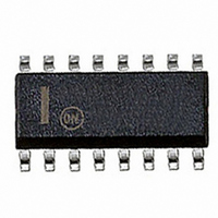
IC MUX QUAD 2INPUT 3ST 16-SOIC

MC74ACT257DR2G

Manufacturer Part Number
MC74ACT257DR2G
Description
IC MUX QUAD 2INPUT 3ST 16-SOIC
Manufacturer
ON Semiconductor
Series
74ACTr
Type
Multiplexerr
Datasheet

Specifications of MC74ACT257DR2G

Circuit
4 x 2:1
Independent Circuits
1
Current - Output High, Low
24mA, 24mA
Voltage Supply Source
Single Supply
Voltage - Supply
4.5 V ~ 5.5 V
Operating Temperature
-40°C ~ 85°C
Mounting Type
Surface Mount
Package / Case
16-SOIC (3.9mm Width)
Logical Function
Mux
Configuration
4 x 2:1
Number Of Inputs
8
Number Of Outputs
4
Operating Supply Voltage (typ)
5V
Operating Supply Voltage (min)
4.5V
Operating Supply Voltage (max)
5.5V
Operating Temp Range
-40C to 85C
Operating Temperature Classification
Industrial
Mounting
Surface Mount
Pin Count
16
Package Type
SOIC
Lead Free Status / RoHS Status
Lead free / RoHS Compliant

Available stocks

Company
Part Number
Manufacturer
Quantity
Price
Part Number:
MC74ACT257DR2G
Manufacturer:
ON/安森美
Quantity:
20 000
MC74AC257, MC74ACT257
Quad 2−Input Multiplexer
with 3−State Outputs
3−state outputs. Four bits of data from two sources can be selected
using a Common Data Select input. The four outputs present the
selected data in true (noninverted) form. The outputs may be switched
to a high impedance state by placing a logic HIGH on the common
Output Enable (OE) input, allowing the outputs to interface directly
with bus−oriented systems.
w
© Semiconductor Components Industries, LLC, 2006
March, 2006 − Rev. 7
Figure 1. Pinout: 16−Lead Packages Conductors
The MC74AC257/74ACT257 is a quad 2−input multiplexer with
These devices are available in Pb−free package(s). Specifications herein
apply to both standard and Pb−free devices. Please see our website at
www.onsemi.com for specific Pb−free orderable part numbers, or
contact your local ON Semiconductor sales office or representative.
Multiplexer Expansion by Tying Outputs Together
Noninverting 3−State Outputs
Outputs Source/Sink 24 mA
′ACT257 Has TTL Compatible Inputs
V
16
S
CC
1
OE
15
I
2
0a
I
14
I
0c
3
1a
(Top View)
I
13
Z
1c
4
a
12
I
Z
5
0b
c
I
I
11
0d
6
1b
I
10
Z
1d
7
b
GND
Z
9
8
d
1
MC74AC257N
MC74ACT257N
MC74AC257D
MC74ACT257D
MC74AC257DR2
MC74ACT257DR2
MC74AC257DT
MC74ACT257DT
MC74AC257DTR2
MC74ACT257DTR2 TSSOP−16
MC74ACT257M
MC74AC257MEL
MC74ACT257MEL
See general marking information in the device marking
section on page 8 of this data sheet.
16
DEVICE MARKING INFORMATION
Device
ORDERING INFORMATION
1
16
16
16
http://onsemi.com
1
1
1
TSSOP−16
TSSOP−16
TSSOP−16
SOIC−16
SOIC−16
Package
SOIC−16
SOIC−16
EIAJ−16
EIAJ−16
EIAJ−16
PDIP−16
PDIP−16
Publication Order Number:
CASE 751B
CASE 948F
DT SUFFIX
TSSOP−16
CASE 648
M SUFFIX
CASE 966
N SUFFIX
D SUFFIX
EIAJ−16
DIP−16
SO−16
2500 Tape & Reel
2500 Tape & Reel
2500 Tape & Reel
2500 Tape & Reel
2000 Tape & Reel
2000 Tape & Reel
MC74AC257/D
25 Units/Rail
25 Units/Rail
48 Units/Rail
48 Units/Rail
96 Units/Rail
96 Units/Rail
50 Units/Rail
Shipping

Related parts for MC74ACT257DR2G

MC74ACT257DR2G Summary of contents

Page 1

... Outputs Source/Sink 24 mA • ′ACT257 Has TTL Compatible Inputs w These devices are available in Pb−free package(s). Specifications herein apply to both standard and Pb−free devices. Please see our website at www.onsemi.com for specific Pb−free orderable part numbers, or contact your local ON Semiconductor sales office or representative ...

Page 2

PIN NAME PIN FUNCTION S Common Data Select Input OE 3−State Output Enable Input I −I Data Inputs from Source −I Data Inputs from Source −Z 3−State Multiplexer Outputs a d TRUTH ...

Page 3

NOTE: This diagram is provided only for the understanding of logic operations and should not be used to estimate propagation delays. Figure 3. Logic Diagram http://onsemi.com I ...

Page 4

MAXIMUM RATINGS* Symbol V DC Supply Voltage (Referenced to GND Input Voltage (Referenced to GND Output Voltage (Referenced to GND) OUT I DC Input Current, per Pin Output Sink/Source Current, per ...

Page 5

DC CHARACTERISTICS Symbol Parameter V Minimum High Level IH Input Voltage V Maximum Low Level IL Input Voltage V Minimum High Level OH Output Voltage V Maximum Low Level OL Output Voltage I Maximum Input IN Leakage Current I Maximum ...

Page 6

... AC CHARACTERISTICS (For Figures and Waveforms − See Section 3 of the ON Semiconductor FACT Data Book, DL138/D) Symbol Parameter Propagation Delay t PLH Propagation Delay t PHL Propagation Delay t PLH Propagation Delay t PHL Output Enable Time PZH t Output Enable Time PZL t Output Disable Time PHZ ...

Page 7

DC CHARACTERISTICS Symbol Parameter V Minimum High Level IH Input Voltage V Maximum Low Level IL Input Voltage V Minimum High Level OH Output Voltage V Maximum Low Level OL Output Voltage I Maximum Input IN Leakage Current DI Additional ...

Page 8

... AC CHARACTERISTICS (For Figures and Waveforms − See Section 3 of the ON Semiconductor FACT Data Book, DL138/D) Symbol Parameter Propagation Delay t PLH Propagation Delay t PHL Propagation Delay t PLH Propagation Delay t PHL Output Enable Time PZH t Output Enable Time PZL t Output Disable Time PHZ ...

Page 9

0.25 (0.010) M −A− −T− SEATING PLANE 0.25 (0.010 PACKAGE DIMENSIONS PDIP−16 N ...

Page 10

K 16X REF 0.10 (0.004) 0.15 (0.006 L PIN 1 IDENT. 1 0.15 (0.006 −V− C 0.10 (0.004) −T− SEATING D PLANE ...

Page 11

Notes http://onsemi.com 11 ...

Page 12

... Fax: 480−829−7709 or 800−344−3867 Toll Free USA/Canada Email: orderlit@onsemi.com N. American Technical Support: 800−282−9855 Toll Free USA/Canada Japan: ON Semiconductor, Japan Customer Focus Center 2−9−1 Kamimeguro, Meguro−ku, Tokyo, Japan 153−0051 Phone: 81−3−5773−3850 http://onsemi.com 12 ON Semiconductor Website: http://onsemi ...

Related keywords