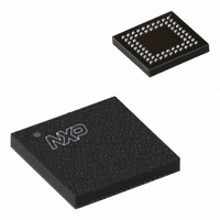
CBTV4010EE,557 NXP Semiconductors, CBTV4010EE,557 Datasheet - Page 4

CBTV4010EE,557
Manufacturer Part Number
CBTV4010EE,557
Description
IC 10BIT 1:4 BUS SWITCH 64-TFBGA
Manufacturer
NXP Semiconductors
Series
CBTr
Type
Bus Switchr
Datasheet
1.CBTV4010EE557.pdf
(10 pages)
Specifications of CBTV4010EE,557
Package / Case
64-TFBGA
Circuit
10 x 1:4
Independent Circuits
1
Voltage Supply Source
Single Supply
Voltage - Supply
2.3 V ~ 2.7 V
Operating Temperature
0°C ~ 85°C
Mounting Type
Surface Mount
Maximum Data Rate
0.4 Gbps
Minimum Operating Temperature
0 C
Mounting Style
SMD/SMT
Number Of Clock Inputs
10
Supply Voltage (max)
2.7 V
Supply Voltage (min)
2.3 V
Maximum Operating Temperature
+ 85 C
Lead Free Status / RoHS Status
Lead free / RoHS Compliant
Current - Output High, Low
-
Lead Free Status / RoHS Status
Lead free / RoHS Compliant, Lead free / RoHS Compliant
Other names
935271264557
CBTV4010EE
CBTV4010EE
CBTV4010EE
CBTV4010EE
Available stocks
Company
Part Number
Manufacturer
Quantity
Price
Company:
Part Number:
CBTV4010EE,557
Manufacturer:
NXP Semiconductors
Quantity:
10 000
1. Stresses beyond those listed may cause permanent damage to the device. These are stress ratings only and functional operation of the
2. The input and output negative-voltage ratings may be exceeded if the input and output clamp-current ratings are observed.
3. The package thermal impedance is calculated in accordance with JESD 51.
1. All unused control inputs of the device must be held at V
Philips Semiconductors
SIMPLIFIED SCHEMATIC, EACH FET SWITCH
ABSOLUTE MAXIMUM RATINGS
NOTES:
RECOMMENDED OPERATING CONDITIONS
NOTE:
2002 Feb 19
SYMBOL
SYMBOL
SYMBOL
10-bit DDR SDRAM mux/bus switch
device at these or any other conditions beyond those indicated under “recommended operating conditions” is not implied. Exposure to
absolute-maximum-rated conditions for extended periods may affect device reliability.
T
V
V
T
V
V
amb
I
V
V
CC
CC
IK
stg
IH
IL
I
I
DC supply voltage
High-level input voltage DIMM port and Host
Low-level Input voltage DIMM port and Host
Operating free-air temperature range
Sn
HPx
A
DC supply voltage
DC input clamp current
DC input voltage range (S pin only)
Storage temperature range
DC input voltage range (except S pin)
PARAMETER
Sw
PARAMETER
PARAMETER
1, 3
2
100
SW00889
nDPx
2
B
CC
or GND to ensure proper device operation.
4
CONDITIONS
LOGIC DIAGRAM (POSITIVE LOGIC)
V
I/O
S0
S1
S2
S3
HP9
< 0
Min
HP0
2.3
1.6
—
0
LIMITS
Typ
2.5
—
—
—
Sw
Sw
Sw
Sw
–0.5 to +3.3
–65 to 150
–0.5 to 3.3
V
RATING
CC
–50
+ 0.3
Sw
Sw
Max
+85
2.7
0.9
—
CBTV4010
Sw
Sw
0DP0
1DP0
2DP0
3DP0
0DP9
1DP9
2DP9
3DP9
SW00901
Product data
UNIT
mA
UNIT
UNIT
V
V
V
C
V
V
V
C


