TC74ACT257P Toshiba, TC74ACT257P Datasheet

IC MULTIPLEXER 2-CH 3-ST 16-DIP

TC74ACT257P

Manufacturer Part Number
TC74ACT257P
Description
IC MULTIPLEXER 2-CH 3-ST 16-DIP
Manufacturer
Toshiba
Series
74ACTr
Type
Multiplexerr
Datasheet

Specifications of TC74ACT257P

Circuit
4 x 2:1
Independent Circuits
1
Current - Output High, Low
24mA, 24mA
Voltage Supply Source
Single Supply
Voltage - Supply
4.5 V ~ 5.5 V
Operating Temperature
-40°C ~ 85°C
Mounting Type
Through Hole
Package / Case
16-DIP (0.300", 7.62mm)
Lead Free Status / RoHS Status
Contains lead / RoHS non-compliant
2-Channel Multiplexer (3-state)
MULTIPLEXER fabricated with silicon gate and double-layer
metal wiring C
Bipolar Schottky TTL while maintaining the CMOS low power
dissipation.
TTL or NMOS to High Speed CMOS. The inputs are compatible
with TTL or NMOS and CMOS output voltage levels.
with common SELECT and
state. When SELECT is set low, “A” data inputs are enabled.
enabled.
discharge or transient excess voltage.
Features
Pin Assignment
The TC74ACT257 is an advanced high speed CMOS
It achieve the high speed operation similar to equivalent
This device may be used as a level converter for interfacing
Each is composed of four independent 2-channel multiplexers
If OE is set low, the outputs are held in a high-impedance
Conversely, when SELECT is high, “B” data inputs are
All inputs are equipped with protection circuits against static
High speed: t
Low power dissipation: I
Compatible with TTL outputs: V
Symmetrical output impedance: |I
Balanced propagation delays: t
Pin and function compatible with 74F257
TC74ACT257P,TC74ACT257F,TC74ACT257FN
2
MOS technology.
pd
= 5.8 ns (typ.) at V
TOSHIBA CMOS Digital Integrated Circuit Silicon Monolithic
CC
OUTPUT
= 8 μA (max) at Ta = 25°C
pLH
V
IL
IH
Capability of driving 50 Ω
transmission lines.
CC
OH
= 0.8 V (max)
ENABLE
∼ − t
= 2.0 V (min)
= 5 V
| = I
pHL
OL
= 24 mA (min)
( OE ).
1
Note:
Weight
DIP16-P-300-2.54A
SOP16-P-300-1.27A
SOL16-P-150-1.27
TC74ACT257P
TC74ACT257F
TC74ACT257FN
xxxFN (JEDEC SOP) is not available in
Japan.
TC74ACT257P/F/FN
: 1.00 g (typ.)
: 0.18 g (typ.)
: 0.13 g (typ.)
2007-10-01

Related parts for TC74ACT257P

TC74ACT257P Summary of contents

Page 1

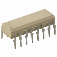
... Pin and function compatible with 74F257 Pin Assignment ENABLE ( 0.8 V (max 2.0 V (min (min Capability of driving 50 Ω transmission lines. ∼ − t pLH pHL 1 TC74ACT257P/F/FN Note: xxxFN (JEDEC SOP) is not available in Japan. TC74ACT257P TC74ACT257F TC74ACT257FN Weight DIP16-P-300-2.54A : 1.00 g (typ.) SOP16-P-300-1.27A : 0.18 g (typ.) SOL16-P-150-1.27 : 0.13 g (typ.) 2007-10-01 ...

Page 2

... IEC Logic Symbol Truth Table Inputs OE SELECT Don’t care Z: High impedance System Diagram Output TC74ACT257P/F/FN 2007-10-01 ...

Page 3

... Unused inputs must be tied to either VCC or GND. Symbol Rating −0 −0 0 −0 0.5 V OUT CC ± ± ±50 I OUT ±100 500 (DIP) (Note 2)/180 (SOP) D −65 to 150 T stg Symbol Rating V 4 OUT CC − opr dt/ TC74ACT257P/F/FN Unit °C Unit °C ns/V 2007-10-01 ...

Page 4

... I /4 (per bit) ・ TC74ACT257P/F/ − 25°C 85°C Min Typ. Max Min Max ⎯ ⎯ 2.0 2.0 ⎯ ⎯ ⎯ 0.8 0.8 ⎯ ...

Page 5

... Package Dimensions Weight: 1.00 g (typ.) TC74ACT257P/F/FN 5 2007-10-01 ...

Page 6

... Package Dimensions Weight: 0.18 g (typ.) TC74ACT257P/F/FN 6 2007-10-01 ...

Page 7

... Package Dimensions (Note) Note: This package is not available in Japan. Weight: 0.13 g (typ.) TC74ACT257P/F/FN 7 2007-10-01 ...

Page 8

... Please contact your TOSHIBA sales representative for details as to environmental matters such as the RoHS compatibility of Product. Please use Product in compliance with all applicable laws and regulations that regulate the inclusion or use of controlled substances, including without limitation, the EU RoHS Directive. TOSHIBA assumes no liability for damages or losses occurring as a result of noncompliance with applicable laws and regulations. TC74ACT257P/F/FN 8 2007-10-01 ...

Related keywords