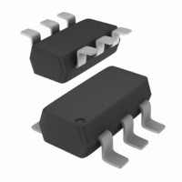
74LVC1GX04GV,125 NXP Semiconductors, 74LVC1GX04GV,125 Datasheet - Page 12

74LVC1GX04GV,125
Manufacturer Part Number
74LVC1GX04GV,125
Description
IC X-TAL DRIVER 6-TSSOP
Manufacturer
NXP Semiconductors
Series
74LVCr
Datasheet
1.74LVC1GX04GV125.pdf
(16 pages)
Specifications of 74LVC1GX04GV,125
Package / Case
SC-74-6
Logic Type
Crystal Oscillator Driver
Supply Voltage
1.65 V ~ 5.5 V
Operating Temperature
-40°C ~ 125°C
Mounting Type
Surface Mount
Supply Voltage (max)
5.5 V
Supply Voltage (min)
1.65 V
Maximum Operating Temperature
+ 125 C
Mounting Style
SMD/SMT
Maximum Power Dissipation
300 mW
Minimum Operating Temperature
- 40 C
Output Current
50 mA
Output Voltage
5.5 V
Lead Free Status / RoHS Status
Lead free / RoHS Compliant
Number Of Bits
-
Lead Free Status / Rohs Status
Lead free / RoHS Compliant
Other names
568-3010-2
935274025125
935274025125
Philips Semiconductors
Design
Figure 10 shows the recommended way to connect a
crystal to the 74LVC1GX04. This circuit is basically a
Pierce oscillator circuit in which the crystal is operating at
its fundamental frequency and is tuned by the parallel load
capacitance of C
crystal. They should be approximately equal. R
drive-limiting resistor and is set to approximately the same
value as the reactance of C
(R
of the rail-to-rail output of X2. This keeps the drive level
into the crystal within drive specifications (the designer
should verify this). Overdriving the crystal can cause
damage.
The resistor R
point of the inverter near mid-supply, operating the
74LVC1GU04 in the high gain linear region. The value of
R
To calculate the values of C
the formula:
C
manufacturer, C
(for the LVC1GX04 this is equal to an input capacitance
of 5 pf).
2003 Aug 13
handbook, halfpage
f
L
1
X-tal driver
is not critical, typically it is set at 1 M .
is the load capacitance as specified by the crystal
= X
C1
). This will result in an input to the crystal of 50%
Fig.10 Crystal oscillator configuration.
C 2
X1
74LVC1GU04
C
f
L
provides negative feedback and sets a bias
portion
Xtal
s
1
=
R f
is the stray capacitance of the circuit
and C
C
------------------- -
C
1
1
+
X2
C 1
2
C
C
. C
74LVC1G04
2
2
1
+
portion
1
1
and C
at the crystal frequency
C
and C
s
Y
2
2
, the designer can use
system load
are in series with the
C sys
MNB103
R sys
1
is the
12
Testing
After the calculations are performed for a particular crystal,
the oscillator circuit should be tested. The following simple
checks will verify the prototype design of a crystal
controlled oscillator circuit. Perform them after laying out
the board:
As the 74LVC1GX04 isolates the system loading, once the
design is optimized, the single layout may work in multiple
applications for any given crystal.
Test the oscillator over worst-case conditions (lowest
supply voltage, worst-case crystal and highest operating
temperature). Adding series and parallel resistors can
simulate a worse case crystal.
Insure that the circuit does not oscillate without the
crystal.
Check the frequency stability over a supply range
greater than that which is likely to occur during normal
operation.
Check that the start up time is within system
requirements.
74LVC1GX04
Product specification


