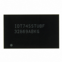
IDT74SSTUBF32869ABKG IDT, Integrated Device Technology Inc, IDT74SSTUBF32869ABKG Datasheet - Page 7

IDT74SSTUBF32869ABKG
Manufacturer Part Number
IDT74SSTUBF32869ABKG
Description
IC BUFFER 14BIT REG DDR2 150-BGA
Manufacturer
IDT, Integrated Device Technology Inc
Datasheet
1.IDT74SSTUBF32869ABKG.pdf
(21 pages)
Specifications of IDT74SSTUBF32869ABKG
Number Of Bits
14
Logic Type
1:2 Registered Buffer with Parity
Supply Voltage
1.7 V ~ 1.9 V
Operating Temperature
0°C ~ 70°C
Mounting Type
Surface Mount
Package / Case
150-CABGA, CTBGA
Logic Family
SSTU
Logical Function
Reg Bfr W/ParityTst
Number Of Elements
1
Number Of Inputs
14
Number Of Outputs
28
High Level Output Current
-12mA
Low Level Output Current
12mA
Propagation Delay Time
3ns
Operating Supply Voltage (typ)
1.8V
Operating Supply Voltage (max)
1.9V
Operating Supply Voltage (min)
1.7V
Clock-edge Trigger Type
Posit/Negat-Edge
Polarity
Non-Inverting
Technology
CMOS
Frequency (max)
340(Min)MHz
Mounting
Surface Mount
Pin Count
150
Operating Temp Range
0C to 70C
Operating Temperature Classification
Commercial
Lead Free Status / RoHS Status
Lead free / RoHS Compliant
Other names
74SSTUBF32869ABKG
800-1697
800-1697
Available stocks
Company
Part Number
Manufacturer
Quantity
Price
Company:
Part Number:
IDT74SSTUBF32869ABKG
Manufacturer:
IDT, Integrated Device Technology Inc
Quantity:
10 000
Company:
Part Number:
IDT74SSTUBF32869ABKG8
Manufacturer:
Skyworks
Quantity:
800
Company:
Part Number:
IDT74SSTUBF32869ABKG8
Manufacturer:
IDT, Integrated Device Technology Inc
Quantity:
10 000
14-BIT CONFIGURABLE REGISTERED BUFFER FOR DDR2
IDT74SSTUBF32869A
14-BIT CONFIGURABLE REGISTERED BUFFER FOR DDR2
Terminal Functions
Miscellaneous
Configuration
Parity Output
Gated Inputs
Clock Inputs
Chip Select
Chip Select
Parity Input
Parity Error
Re-Driven
Ungated
1
Outputs
Signal
Group
Output
Inputs
Inputs
Inputs
Inputs
This range does not include D1, D4, and D7, and their corresponding outputs.
DCKE, DODT
Q1A...Q14A
Q1B...Q14B
QODTnA, B
QCKEnA, B
DCS, CSR
QCSnA, B
Terminal
D1...D14
CLK, CLK
PTYERR
RESET
Name
PARIN
V
PPO
GND
V
C1
REF
DD
1
1
1
,
,
0.9V nominal
Ground Input Ground
Power Input
Open Drain
SSTL_18
SSTL_18
SSTL_18
SSTL_18
SSTL_18
SSTL_18
SSTL_18
SSTL_18
SSTL_18
Type
Input
DRAM function pins not associated with Chip Select
DRAM inputs, re-driven only when Chip Select is LOW
DRAM Chip Select signals. These pins initiate DRAM
address/command decodes, and as such at least one will be
LOW when a valid address/command is present.
Outputs of the register, valid after the specified clock count and
immediately following a rising edge of the clock
Input parity is received on pin PARIN, and should maintain odd
parity across the D1:D14 inputs, at the rising edge of the clock,
one cycle after Chip Select is LOW.
Partial Parity Output. Indicates parity out of D1-D14.
When LOW, this output indicates that a parity error was
identified associated with the address and/or command inputs.
PTYERR will be active for two clock cycles, and delayed by in
total two clock cycles for compatibility with final parity out timing
on the industry-standard DDR2 register with parity (in JEDEC
definition).
When LOW, the register is configured as Register 1. When
HIGH, the register is configured as Register 2.
Differential master clock input pair to the register. The register
operation is triggered by a rising edge on the positive clock
input (CLK).
Asynchronous Reset Input. When LOW, it causes a reset of the
internal latches, thereby forcing the outputs LOW. RESET also
resets the PTYERR signal.
Input reference voltage for SSTL_18 inputs. Two pins
(internally tied together) are used for increased
Inputsreliability.
Power Supply Voltage
7
CONFIDENTIAL
COMMERCIAL TEMPERATURE GRADE
Description
IDT74SSTUBF32869A
7093/10


