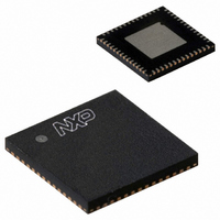
SSTVF16859BS,118 NXP Semiconductors, SSTVF16859BS,118 Datasheet - Page 11

SSTVF16859BS,118
Manufacturer Part Number
SSTVF16859BS,118
Description
IC REG BUFF 13BIT SSTL 56HVQFN
Manufacturer
NXP Semiconductors
Series
74SSTVFr
Datasheet
1.SSTVF16859BS118.pdf
(23 pages)
Specifications of SSTVF16859BS,118
Logic Type
Registered Buffer for DDR
Package / Case
56-VQFN Exposed Pad, 56-HVQFN, 56-SQFN, 56-DHVQFN
Supply Voltage
2.3 V ~ 2.7 V
Number Of Bits
13, 26
Operating Temperature
0°C ~ 70°C
Mounting Type
Surface Mount
Logic Family
SSTV
Number Of Circuits
1
Maximum Clock Frequency
210 MHz
Propagation Delay Time
1.7 ns
High Level Output Current
- 16 mA
Low Level Output Current
16 mA
Supply Voltage (max)
2.7 V
Maximum Operating Temperature
+ 70 C
Minimum Operating Temperature
0 C
Mounting Style
SMD/SMT
Supply Voltage (min)
2.3 V
Lead Free Status / RoHS Status
Lead free / RoHS Compliant
Lead Free Status / RoHS Status
Lead free / RoHS Compliant, Lead free / RoHS Compliant
Other names
568-2055-2
935276956118
SSTVF16859BS-T
935276956118
SSTVF16859BS-T
Philips Semiconductors
11. Dynamic characteristics
Table 9:
At recommended operating conditions; V
See
[1]
[2]
[3]
[4]
[5]
[6]
Table 10:
At recommended operating conditions; V
See
[1]
[2]
[3]
[4]
[5]
[6]
9397 750 15157
Product data sheet
Symbol
f
t
t
t
t
t
Symbol
f
t
t
t
t
t
clock
W
ACT
INACT
su
h
clock
W
ACT
INACT
su
h
This parameter is not necessarily production tested.
Data inputs must be below a minimum time to t
Data and clock inputs must be held at valid levels (not floating) a minimum time of t
For data signal input slew rate
For data signal input slew rate
CK, CK signals input slew rates are
This parameter is not necessarily production tested.
Data inputs must be below a minimum time to t
Data and clock inputs must be held at valid levels (not floating) a minimum time of t
For data signal input slew rate
For data signal input slew rate
CK, CK signals input slew rates are
Figure
Figure
11.
11.
Timing requirements (PC1600-PC2700)
Timing requirements (PC3200)
Parameter
clock frequency
pulse duration, CK, CK, HIGH or
LOW
differential inputs active time
differential inputs inactive time
setup time, fast slew rate
setup time, slow slew rate
hold time, fast slew rate
hold time, slow slew rate
Parameter
clock frequency
pulse duration, CK, CK, HIGH or
LOW
differential inputs active time
differential inputs inactive time
setup time, fast slew rate
setup time, slow slew rate
hold time, fast slew rate
hold time, slow slew rate
1 V/ns.
0.5 V/ns and < 1 V/ns.
1 V/ns.
0.5 V/ns and < 1 V/ns.
1 V/ns.
1 V/ns.
DD
DD
= 2.5 V
= 2.6 V
ACT(max)
ACT(max)
Rev. 02 — 19 July 2005
, after RESET is taken HIGH.
, after RESET is taken HIGH.
Conditions
data before CK , CK
data before CK , CK
data after CK , CK
data after CK , CK
Conditions
data before CK , CK
data before CK , CK
data after CK , CK
data after CK , CK
0.2 V; T
0.1 V; T
amb
amb
= 0 C to +70 C; unless otherwise specified.
= 0 C to +70 C; unless otherwise specified.
13-bit 1 : 2 SSTL_2 registered buffer for DDR
INACT(max)
INACT(max)
[1] [2]
[1] [3]
[4] [6]
[5] [6]
[4] [6]
[5] [6]
[1] [2]
[1] [3]
[4] [6]
[5] [6]
[4] [6]
[5] [6]
Min
-
2.5
-
-
0.65
0.75
0.75
0.9
Min
-
2.5
-
-
0.65
0.75
0.65
0.8
, after RESET is taken LOW.
, after RESET is taken LOW.
© Koninklijke Philips Electronics N.V. 2005. All rights reserved.
SSTVF16859
Typ
-
-
-
-
-
-
-
-
Typ
-
-
-
-
-
-
-
-
Max
200
-
22
22
-
-
-
-
Max
210
-
22
22
-
-
-
-
Unit
MHz
ns
ns
ns
ns
ns
ns
ns
Unit
MHz
ns
ns
ns
ns
ns
ns
ns
11 of 23


