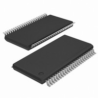
SSTV16857CG IDT, Integrated Device Technology Inc, SSTV16857CG Datasheet - Page 3

SSTV16857CG
Manufacturer Part Number
SSTV16857CG
Description
IC REGIST BUFF 14BIT DDR 48TSSOP
Manufacturer
IDT, Integrated Device Technology Inc
Series
74SSTVr
Datasheet
1.SSTV16857CGT.pdf
(9 pages)
Specifications of SSTV16857CG
Number Of Bits
14
Logic Type
Registered Buffer with SSTL_2 Inputs and Outputs
Supply Voltage
2.3 V ~ 2.7 V
Operating Temperature
-40°C ~ 85°C
Mounting Type
Surface Mount
Package / Case
48-TSSOP
Logic Family
SSTV
Logical Function
Registered Buffer
Number Of Elements
1
Number Of Inputs
14
Number Of Outputs
14
High Level Output Current
-20mA
Low Level Output Current
20mA
Propagation Delay Time
3.5ns
Operating Supply Voltage (typ)
2.5V
Operating Supply Voltage (max)
2.7V
Operating Supply Voltage (min)
2.3V
Clock-edge Trigger Type
Posit/Negat-Edge
Polarity
Non-Inverting
Technology
CMOS
Frequency (max)
200(Min)MHz
Mounting
Surface Mount
Pin Count
48
Operating Temp Range
0C to 70C
Operating Temperature Classification
Commercial
Lead Free Status / RoHS Status
Contains lead / RoHS non-compliant
Available stocks
Company
Part Number
Manufacturer
Quantity
Price
Company:
Part Number:
SSTV16857CG
Manufacturer:
ICS
Quantity:
35 196
IDT™ / ICS™ DDR 14-Bit Registered Buffer
ICSSSTV16857C
DDR 14-Bit Registered Buffer
0002F—10/25/02
Stresses above those listed under Absolute Maximum Ratings may cause permanent damage to the device. These ratings
are stress specifications only and functional operation of the device at these or any other conditions above those listed in
the operational sections of the specifications is not implied. Exposure to absolute maximum rating conditions for extended
periods may affect product reliability.
1
Recommended Operating Conditions
Absolute Maximum Ratings
PARAMETER
Guarenteed by design, not 100% tested in production.
V
V
V
V
Storage Temperature . . . . . . . . . . . . . . . . . . . . –65°C to +150°C
Supply Voltage . . . . . . . . . . . . . . . . . . . . . . . . . -0.5 to 3.6V
Input Voltage
Output Voltage
Input Clamp Current . . . . . . . . . . . . . . . . . . . . ±50 mA
Output Clamp Current . . . . . . . . . . . . . . . . . . . ±50 mA
Continuous Output Current . . . . . . . . . . . . . . . ±50 mA
V
Package Thermal Impedance
V
V
V
DD
V
IH (DC)
IH (AC)
IL (DC)
IL (DC)
V
V
V
V
V
I
I
T
V
DDQ
REF
OH
OL
ICR
DD
TT
IH
ID
IX
IL
A
I
, V
DDQ
or GND Current/Pin . . . . . . . . . . . . ±100 mA
Supply Voltage
I/O Supply Voltage
Reference Voltage
Termination Voltage
Input Voltage
DC Input High Voltage
AC Input High Voltage
DC Input Low Voltage
AC Input Low Voltage
Input High Voltage Level
Input Low Voltage Level
Common mode Input Range
Differential Input Voltage
Cross Point Voltage of Differential Clock
Pair
High-Level Output Current
Low-Level Output Current
Operating Free-Air Temperature
1
. . . . . . . . . . . . . . . . . . . . . . . . . . . . . . . . .
1,2
. . . . . . . . . . . . . . . . . . . . . . . . . . . . . .
DESCRIPTION
3
. . . . . . . . . . . . . . . .
Data Inputs
RESET#
CLK, CLK#
-0.5 to V
-0.5 to V
55°C/W
3
3
DD
DDQ
(V
V
V
V
DDQ
REF
REF
+0.5
REF
+0.5
1.15
0.97
0.36
MIN
2.3
2.3
1.7
/2) - 0.2
0
+ 0.15
+ 0.31
0
- 0.04
Notes:
1. The input and output negative voltage
2. This current will flow only when the
3. The package thermal impedance is
TYP
1.25
V
2.5
2.5
REF
ratings may be excluded if the input
and output clamp ratings are observed.
output is in the high state level
V
calculated in accordance with
JESD 51.
0
>V
DDQ
(V
V
V
V
DDQ
.
REF
REF
REF
MAX
V
1.35
1.53
2.7
2.7
0.7
/2) + 0.2
-20
20
70
DDQ
+ 0.04
- 0.15
- 0.31
UNITS
mA
°C
V
ICSSSTV16857C
TSD


