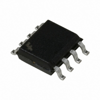
100LVEL16MX Fairchild Semiconductor, 100LVEL16MX Datasheet - Page 3

100LVEL16MX
Manufacturer Part Number
100LVEL16MX
Description
IC RECEIVER 3.3V ECL DIFF 8SOIC
Manufacturer
Fairchild Semiconductor
Series
100LVELr
Datasheet
1.100LVEL16M.pdf
(6 pages)
Specifications of 100LVEL16MX
Logic Type
ECL Differential Receiver
Supply Voltage
3 V ~ 3.8 V
Number Of Bits
1
Operating Temperature
-40°C ~ 85°C
Mounting Type
Surface Mount
Package / Case
8-SOIC (3.9mm Width)
Logic Family
100LV
Supply Voltage (max)
3.8 V
Supply Voltage (min)
3 V
Maximum Operating Temperature
+ 85 C
Mounting Style
SMD/SMT
Interface
EIA/JESD78
Minimum Operating Temperature
- 40 C
Number Of Lines (input / Output)
/ /
Supply Current
24 mA
Lead Free Status / RoHS Status
Lead free / RoHS Compliant
I
V
V
V
V
V
V
I
I
f
t
t
t
V
t
EE
IH
IL
MAX
PLH
SKEW
JITTER
r
LVNECL DC Electrical Characteristics
Note 6: Input and output parameters vary 1 to 1 with V
Note 7: Outputs are terminated through a 50 Resistor to V
Note 8: V
differential input signal. Normal operation is obtained if the HIGH level falls within the specified range and the peak-to-peak voltage lies between V
1V.
Note 9: Absolute value of the input HIGH and LOW current should not exceed the absolute value of the stated Min or Max specification.
Note: Devices are designed to meet the DC specifications after thermal equilibrium has been established. Circuit is tested with air flow greater than
500LFPM maintained.
100LVEL16 AC Electrical Characteristics
(Note 10) (Note 11)
Note 10: V
Note 11: Measured using a 750 mV input swing centered at V
with 50
Note 12: Duty cycle skew is the difference between a t
Symbol
Symbol
, t
OH
OL
IH
IL
BB
IHCMR
PP
f
, t
PHL
to V
IHCMR
EE
Power Supply Current
Output HIGH Voltage (Note 7)
Output LOW Voltage (Note 7)
Input HIGH Voltage (Single Ended)
Input LOW Voltage (Single Ended)
Output Voltage Reference
Input HIGH Voltage Common Mode
Range (Differential) (Note 8)
Input HIGH Current
Input LOW Current
Maximum Toggle Frequency
Propagation Delay to Output (Diff)
Duty Cycle Skew (Note 12)
Cycle-to-Cycle Jitter
Input Swing
Output Rise Times Q (20% to 80%)
CC
can vary
minimum varies 1 to 1 with V
2.0V.
0.3V.
Parameter
Parameter
V
V
PP
PP
500mV
500mV
(SE)
EE
. V
D
D
IHCMR
CC
PLH
Min
150
100
150
120
Min
1085
1830
1165
1810
1.38
0.5
600
. V
2.5
1.8
maximum varies 1-to-1 with V
and t
EE
CC
CC
can vary 0.3V.
PHL
TBD
TBD
40 C
Typ
275
275
220
- 1.32V; 50% duty cycle clock source; t
2.0V.
5
40 C
Typ
1005
1695
17
propagation delay through a device under identical conditions.
1000
Max
400
450
320
30
Max
1555
1475
150
1.26
3
23
880
880
0.4
0.4
V
CC
Min
225
175
150
120
CC
V
Min
1025
1810
1810
1165
1.38
0.5
600
2.5
1.9
CC
. The V
0.0V; V
25 C
TBD
TBD
Typ
300
300
220
5
3.3V; V
IHCMR
25 C
Typ
1705
EE
17
955
r
1000
Max
375
425
320
range is referenced to the most positive side of the
20
EE
t
f
3.3V (Note 6)
Max
1620
1475
150
250 ps (20% - 80%) at f
1.26
23
880
880
0.4
0.4
0.0V or V
Min
240
190
150
120
Min
1025
1810
1810
1165
1.38
0.5
600
2.5
1.9
85 C
TBD
TBD
Typ
315
315
220
CC
5
85 C
www.fairchildsemi.com
Typ
1705
18
955
0.0V; V
1000
Max
IN
390
440
320
20
1 MHz. All loading
-1475
EE
Max
Units
1620
150
GHz
1.26
880
880
24
mV
0.4
0.4
ps
ps
ps
ps
PPMIN
Number
3.3V
Figure 1
Figure 2
Figures
Figure
Units
and
1, 3
mV
mA
mV
mV
mV
V
V
A
A


