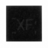
FXLA102L8X Fairchild Semiconductor, FXLA102L8X Datasheet

FXLA102L8X
Specifications of FXLA102L8X
Available stocks
Related parts for FXLA102L8X
FXLA102L8X Summary of contents
Page 1
... Mil Std 883e 3015.7) - 2kV CDM (per ESD STM 5.3) Ordering Information Operating Top Part Number Temperature Mark FXLA102L8X XF -40 to 85°C © 2009 Fairchild Semiconductor Corporation FXLA102 • Rev. 1.0.2 Description The FXLA102 is a configurable dual-voltage supply translator for both uni-directional and bi-directional voltage translation between two logic levels ...
Page 2
... A A Side Input or 3-State Output 1 4 GND Ground 5 /OE Output Enable Input Side Input or 3-State Output Side Input or 3-State Output Side Power Supply CCB © 2009 Fairchild Semiconductor Corporation FLXA102 • Rev. 1.0 CCA 0 Figure 1. Pin Configuration (Top Through View GND ...
Page 3
... Functional Diagram Function Table Control / HIGH Logic Level L = LOW Logic Level © 2009 Fairchild Semiconductor Corporation FLXA102 • Rev. 1.0 CCA CCB Figure 2. Functional Diagram Outputs Normal Operation 3-State www.fairchildsemi.com ...
Page 4
... Input Voltage IN Dynamic Output Current I Static Output Current T Operating Temperature, Free Air A dt/dV Maximum Input Edge Rate Thermal Resistance JA © 2009 Fairchild Semiconductor Corporation FLXA102 • Rev. 1.0.2 Conditions V CCA V CCB I/O Ports A and B Control Input (/OE) Output 3-State Output Active (A ) ...
Page 5
... The recommended power-up sequence is: 1. Apply power to the first Apply power to the second V 3. Drive the /OE input LOW to enable the device. © 2009 Fairchild Semiconductor Corporation FLXA102 • Rev. 1.0.2 The recommended power-down sequence is Drive /OE input HIGH to disable the device. 2. Remove power from either V 3. ...
Page 6
... Voltage V OHB V Low-Level Output OLA (3) Voltage V OLB Bus-Hold Input Minimum I I(HOLD) Drive Current © 2009 Fairchild Semiconductor Corporation FLXA102 • Rev. 1.0.2 Conditions V (V) V CCA CCB 2.70 to 3.60 2.30 to 2.70 Data Inputs A n 1.65 to 2.30 1.10 to 3.60 Control Pin /OE 1.40 to 1.65 1 ...
Page 7
... An external drive must source at least the specified current to switch LOW-to-HIGH external drive must source at least the specified current to switch HIGH-to-LOW the V associated with the input side. CCI CC 7. Reflects current per supply, V © 2009 Fairchild Semiconductor Corporation FLXA102 • Rev. 1.0.2 (Continued) Conditions V (V) CCA 3.60 2.70 Data Inputs ...
Page 8
... Dynamic Output I +12.0 OLD Current (10) Low Notes: 8. Dynamic output characteristics are guaranteed, but not tested. 9. See Figure 7. 10. See Figure 8. © 2009 Fairchild Semiconductor Corporation FLXA102 • Rev. 1.0.2 =4pF), T =-40 to 85°C I/O A =3.0V V =2.3V V =1.65V CCA CCA to 2.7V to 1.95V Max ...
Page 9
... Skew is the variation of propagation delay between output signals and applies only to output signals on the same port ( and switching with the same polarity (LOW-to-HIGH or HIGH-to-LOW) (see Figure 10 Skew is guaranteed, but not tested. © 2009 Fairchild Semiconductor Corporation FLXA102 • Rev. 1.0.2 =3.0V V =2.3V V =1.65V ...
Page 10
... Skew is the variation of propagation delay between output signals and applies only to output signals on the same port ( and switching with the same polarity (LOW-to-HIGH or HIGH-to-LOW) (see Figure 10 Skew is guaranteed, but not tested. © 2009 Fairchild Semiconductor Corporation FLXA102 • Rev. 1.0.2 =3.0V V =2.3V V =1.65V ...
Page 11
... Maximum data rate is specified in megabits per second (see Figure 9 equivalent to two times the F-toggle frequency, specified in megahertz. For example, 100Mbps is equivalent to 50MHz. Capacitance Symbol Parameter C Input Capacitance Control Pin (/OE Input / Output Capacitance I/O C Power Dissipation Capacitance pd © 2009 Fairchild Semiconductor Corporation FLXA102 • Rev. 1.0.2 V =2.3V V =1.65V V CCB CCB CCB to 2.7V to 1.95V to 1.6V Min. ...
Page 12
... This weak driver is called the “bus hold.” “Static Mode” is when only the bus hold drives the channel. The © 2009 Fairchild Semiconductor Corporation FLXA102 • Rev. 1.0.2 bus hold can be over ridden in the event of a direction change ...
Page 13
... Figure 4. Waveform for Inverting and Non-Inverting Functions Notes: 15. Input 2.0ns, 10 16. Input 2.5ns, 10 © 2009 Fairchild Semiconductor Corporation FLXA102 • Rev. 1.0 TEST DUT SIGNAL C1 Figure 3. Test Circuit Input Signal Data Pulses 0V V CCI ...
Page 14
... Test Measure Points Symbol (21 Note: 21 for control pin / CCI CCA © 2009 Fairchild Semiconductor Corporation FLXA102 • Rev. 1.0.2 Figure 5. 3-State Output Low Enable Time = 3.0V to 3.6V only. I Figure 6. 3-State Output High Enable Time = 3.0V to 3.6V only. I =(V /2). MI CCA CCI ...
Page 15
... Figure 7. Active Output Rise Time and Dynamic Output Current High V OLD Figure 8. DATA DATA OUTPUT DATA OUTPUT Note: 22 – SKEW pHLmax pHLmin © 2009 Fairchild Semiconductor Corporation FLXA102 • Rev. 1.0.2 t rise 80 OUT 20 CCO V OL Time V OUT ( ...
Page 16
... Package drawings are provided as a service to customers considering Fairchild components. Drawings may change in any manner without notice. Please note the revision and/or date on the drawing and contact a Fairchild Semiconductor representative to verify or obtain the most recent revision. Package specifications do not expand the terms of Fairchild’s worldwide terms and conditions, specifically the warranty therein, which covers Fairchild products. Always visit Fairchild Semiconductor’ ...
Page 17
... Fairchild Semiconductor Corporation FLXA102 • Rev. 1.0.2 17 www.fairchildsemi.com ...


