74LVXC3245WM Fairchild Semiconductor, 74LVXC3245WM Datasheet

IC TRANSCEIVER 8BIT 4SOIC

74LVXC3245WM

Manufacturer Part Number
74LVXC3245WM
Description
IC TRANSCEIVER 8BIT 4SOIC
Manufacturer
Fairchild Semiconductor
Series
74LVXCr
Datasheet

Specifications of 74LVXC3245WM

Logic Function
Translator, 3-State
Number Of Bits
8
Input Type
TTL
Output Type
Logic
Number Of Channels
8
Number Of Outputs/channel
1
Differential - Input:output
No/No
Propagation Delay (max)
4.8ns
Voltage - Supply
2.7 V ~ 3.6 V, 3 V ~ 5.5 V
Operating Temperature
-40°C ~ 85°C
Package / Case
24-SOIC (7.5mm Width)
Supply Voltage
*
Logic Type
CMOS
Logic Family
74LVX
Number Of Channels Per Chip
8
Input Level
CMOS
Output Level
CMOS
High Level Output Current
- 24 mA
Low Level Output Current
24 mA
Propagation Delay Time
8.5 ns
Supply Voltage (max)
3.6 V, 5.5 V
Supply Voltage (min)
2.7 V, 3 V
Maximum Operating Temperature
+ 85 C
Function
Transceiver
Input Bias Current (max)
8 uA
Minimum Operating Temperature
- 40 C
Mounting Style
SMD/SMT
Number Of Circuits
2
Polarity
Non-Inverting
Logic Device Type
Transceiver, Non Inverting
Supply Voltage Range
2.7V To 3.6V, 3V To 5.5V
Logic Case Style
SOIC
No. Of Pins
24
Operating Temperature Range
-40°C To +85°C
Family Type
LVXC
Rohs Compliant
Yes
Lead Free Status / RoHS Status
Lead free / RoHS Compliant
Data Rate
-
Lead Free Status / Rohs Status
Lead free / RoHS Compliant
© 1994 Fairchild Semiconductor Corporation
74LVXC3245WM
74LVXC3245QSC
74LVXC3245MTC
74LVXC3245
8-Bit Dual Supply Configurable Voltage Interface
Transceiver with 3-STATE Outputs
Features
■ Bidirectional interface between 3V and 3V-to-5V buses
■ Control inputs compatible with TTL level
■ Outputs source/sink up to 24 mA
■ Guaranteed simultaneous switching noise level and
■ Implements patented EMI reduction circuitry
■ Flexible V
■ Allows B Port and V
■ Functionally compatible with the 74 series 245
Ordering Code:
Devices also available in Tape and Reel. Specify by appending suffix letter “X” to the ordering code.
Logic Symbol/s
Pin Descriptions
Order Number
dynamic threshold performance
is HIGH
Pin Names
A
B
T/R
OE
0
0
–A
–B
7
7
CCB
operating range
Output Enable Input
Transmit/Receive Input
Side A Inputs or 3-STATE Outputs
Side B Inputs or 3-STATE Outputs
Package Number
CCB
MQA24
MTC24
M24B
to float simultaneously when OE
Description
224-Lead Small Outline Integrated Circuit (SOIC), JEDEC MS-013, 0.300" Wide
24-Lead Quarter Size Outline Package (QSOP), JEDEC MO-137, 0.150" Wide
24-Lead Thin Shrink Small Outline Package (TSSOP), JEDEC MO-153, 4.4mm Wide
General Description
The LVXC3245 is a 24-pin dual-supply, 8-bit configurable
voltage interface transceiver suited for PCMCIA and other
real time configurable I/O applications. The V
accepts a 3V supply level. The A Port is a dedicated 3V
port. The V
Port is configured to track the V
tively. A 5V level on the V
at a 5V level and a 3V V
3V level. The A Port should interface with a 3V host system
and the B Port to the card slots. This device will allow the
V
when OE is HIGH. This feature is necessary to buffer data
to and from a PCMCIA socket that permits PCMCIA cards
to be inserted and removed during normal operation.
Connection Diagram/s
CCB
voltage source pin and I/O pins on the B Port to float
Package Description
CCB
pin accepts a 3V-to-5V supply level. The B
CC
CC
will configure the I/O pins at a
pin will configure the I/O pins
CCB
supply level respec-
www.fairchildsemi.com
February 2009
CCA
pin

Related parts for 74LVXC3245WM

74LVXC3245WM Summary of contents

Page 1

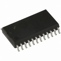
... OE CCB is HIGH ■ Functionally compatible with the 74 series 245 Ordering Code: Order Number Package Number 74LVXC3245WM M24B 224-Lead Small Outline Integrated Circuit (SOIC), JEDEC MS-013, 0.300" Wide 74LVXC3245QSC MQA24 24-Lead Quarter Size Outline Package (QSOP), JEDEC MO-137, 0.150" Wide 74LVXC3245MTC MTC24 24-Lead Thin Shrink Small Outline Package (TSSOP), JEDEC MO-153, 4 ...

Page 2

Truth Table HIGH Voltage Level L = LOW Voltage Level X = Immaterial Logic Diagram/s www.fairchildsemi.com Inputs Outputs T/R L Bus B Data to Bus A H Bus A Data to Bus B X ...

Page 3

Absolute Maximum Ratings Supply Voltage ( CCA CCB −0. Input Voltage ( OE, T Input/Output Voltage (V ) I/O −0. −0. ...

Page 4

DC Electrical Characteristics V CCA Symbol Parameter (V) I Maximum 3-STATE 3.6 OZA Output Leakage 3 Maximum 3-STATE 3.6 OZB Output Leakage 3 Maximum B 3 /Input All Inputs ...

Page 5

AC Electrical Characteristics 2.7V–3.6V CCA Symbol Parameter V 4.5V–5.5V CCB Min Typ (Note 6) t Propagation Delay 1.0 4.8 PHL 1.0 3.9 PLH t Propagation Delay 1.0 ...

Page 6

Power Up Considerations To insure the system does not experience unnecessary I current draw, bus contention, or oscillations during power up, the following guidelines should be adhered to (refer to Table 1): • Power up the control side of the ...

Page 7

Physical Dimensions inches (millimeters) unless otherwise noted 24-Lead Small Outline Integrated Circuit (SOIC), JEDEC MS-013, 0.300" Wide 24-Lead Quarter Size Outline Package (QSOP), JEDEC MO-137, 0.150" Wide Package Number M24B Package Number MQA24 7 www.fairchildsemi.com ...

Page 8

Physical Dimensions inches (millimeters) unless otherwise noted (Continued) 24-Lead Thin Shrink Small Outline Package (TSSOP), JEDEC MO-153, 4.4mm Wide Fairchild does not assume any responsibility for use of any circuitry described, no circuit patent licenses are implied and Fairchild reserves ...

Page 9

9 www.fairchildsemi.com ...

Related keywords