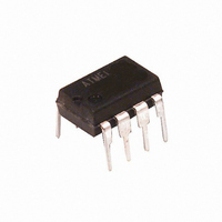
AT93C46D-PU Atmel, AT93C46D-PU Datasheet - Page 5

AT93C46D-PU
Manufacturer Part Number
AT93C46D-PU
Description
IC EEPROM 1KBIT 2MHZ 8DIP
Manufacturer
Atmel
Specifications of AT93C46D-PU
Format - Memory
EEPROMs - Serial
Memory Type
EEPROM
Memory Size
1K (128 x 8 or 64 x 16)
Speed
250kHz, 1MHz, 2MHz
Interface
3-Wire Serial
Voltage - Supply
1.8 V ~ 5.5 V
Operating Temperature
-40°C ~ 85°C
Package / Case
8-DIP (0.300", 7.62mm)
Organization
128 K x 8 or 64 K x 16
Interface Type
3-Wire
Maximum Clock Frequency
2 MHz
Supply Voltage (max)
5.5 V
Supply Voltage (min)
1.8 V
Maximum Operating Current
2 mA
Maximum Operating Temperature
+ 85 C
Mounting Style
Through Hole
Minimum Operating Temperature
- 40 C
Operating Supply Voltage
1.8 V, 5.5 V
Capacitance, Input
5 pF
Capacitance, Output
5 pF
Current, Input, Leakage
0.1 μA
Current, Operating
2 mA
Current, Output, Leakage
0.1
Data Retention
100 yrs.
Density
1K
Package Type
PDIP
Temperature, Operating
-40 to +85 °C
Time, Address Setup
200
Time, Fall
1000 ns
Time, Rise
1000 ns
Voltage, Input, High
2.8 to 6.5 V
Voltage, Input, Low
0.54 to 1.65 V
Voltage, Output, High
1.6 V
Voltage, Output, Low
0.2 V
Voltage, Supply
1.8 to 5.5 V
Memory Configuration
128 X 8, 64 X 16
Clock Frequency
2MHz
Supply Voltage Range
1.8V To 5.5V
Memory Case Style
DIP
No. Of Pins
8
Rohs Compliant
Yes
Lead Free Status / RoHS Status
Lead free / RoHS Compliant
Available stocks
Company
Part Number
Manufacturer
Quantity
Price
Company:
Part Number:
AT93C46D-PU
Manufacturer:
ATMEL
Quantity:
500
Company:
Part Number:
AT93C46D-PU
Manufacturer:
ATMEL
Quantity:
4 500
Part Number:
AT93C46D-PU
Manufacturer:
ATMEL
Quantity:
20 000
Table 1-4.
Note:
2. Functional Description
5193F–SEEPR–1/08
Instruction
READ
EWEN
ERASE
WRITE
ERAL
WRAL
EWDS
The Xs in the address field represent DON’T CARE values and must be clocked.
Instruction Set for the AT93C46D
SB
1
1
1
1
1
1
1
Code
Op
10
00
11
01
00
00
00
The AT93C46D is accessed via a simple and versatile three-wire serial communication inter-
face. Device operation is controlled by seven instructions issued by the host processor. A valid
instruction starts with a rising edge of CS and consists of a start bit (logic “1”) followed by the
appropriate op code and the desired memory address location.
READ (READ): The Read (READ) instruction contains the address code for the memory loca-
tion to be read. After the instruction and address are decoded, data from the selected memory
location is available at the serial output pin DO. Output data changes are synchronized with the
rising edges of serial clock SK. It should be noted that a dummy bit (logic “0”) precedes the 8- or
16-bit data output string.
ERASE/WRITE ENABLE (EWEN): To assure data integrity, the part automatically goes into the
Erase/Write Disable (EWDS) state when power is first applied. An Erase/Write Enable (EWEN)
instruction must be executed first before any programming instructions can be carried out.
Please note that once in the EWEN state, programming remains enabled until an EWDS instruc-
tion is executed or V
ERASE (ERASE): The Erase (ERASE) instruction programs all bits in the specified memory
location to the logical “1” state. The self-timed erase cycle starts once the Erase instruction and
address are decoded. The DO pin outputs the Ready/Busy status of the part if CS is brought
high after being kept low for a minimum of 250 ns (t
selected memory location has been erased and the part is ready for another instruction.
WRITE (WRITE): The Write (WRITE) instruction contains the 8 or 16 bits of data to be written
into the specified memory location. The self-timed programming cycle t
of data is received at serial data input pin DI. The DO pin outputs the Read/Busy status of the
part if CS is brought high after being kept low for a minimum of 250 ns (t
indicates that programming is still in progress. A logic “1” indicates that the memory location at
the specified address has been written with the data pattern contained in the instruction and the
11XXXXX
10XXXXX
01XXXXX
00XXXXX
A
A
A
6
6
6
x 8
– A
– A
– A
0
0
0
Address
CC
11XXXX
10XXXX
01XXXX
00XXXX
A
A
A
power is removed from the part.
x 16
5
5
5
– A
– A
– A
0
0
0
D
D
7
7
x 8
– D
– D
0
0
Data
D
D
15
15
x 16
– D
– D
CS
). A logic “1” at pin DO indicates that the
0
0
Comments
Reads data stored in memory, at
specified address
Write enable must precede all
programming modes
Erases memory location A
Writes memory location A
Erases all memory locations. Valid
only at V
Writes all memory locations. Valid
only at V
Disables all programming instructions
CC
CC
= 4.5V to 5.5V
= 4.5V to 5.5V
WP
starts after the last bit
CS
AT93C46D
). A logic “0” at DO
n
n
– A
– A
0
0
5


