23K256-I/P Microchip Technology, 23K256-I/P Datasheet - Page 13
23K256-I/P
Manufacturer Part Number
23K256-I/P
Description
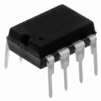
IC SRAM 256KBIT 20MHZ 8DIP
Manufacturer
Microchip Technology
Type
Synchronousr
Specifications of 23K256-I/P
Memory Size
256K (32K x 8)
Package / Case
8-DIP (0.300", 7.62mm)
Format - Memory
RAM
Memory Type
SRAM
Speed
20MHz
Interface
SPI Serial
Voltage - Supply
2.7 V ~ 3.6 V
Operating Temperature
-40°C ~ 85°C
Access Time
25 ns
Maximum Clock Frequency
20 MHz
Supply Voltage (max)
3.6 V
Supply Voltage (min)
2.7 V
Maximum Operating Current
10 mA
Maximum Operating Temperature
+ 85 C
Minimum Operating Temperature
- 40 C
Mounting Style
Through Hole
Number Of Ports
1
Operating Supply Voltage
3.3 V
Lead Free Status / RoHS Status
Lead free / RoHS Compliant
Lead Free Status / RoHS Status
Lead free / RoHS Compliant, Lead free / RoHS Compliant
Available stocks
Company
Part Number
Manufacturer
Quantity
Price
Company:

Part Number:
23K256-I/P
Manufacturer:
MCP
Quantity:
60
Company:
Part Number:
23K256-I/P
Manufacturer:
MICROCHIP
Quantity:
12 000


3.0
The descriptions of the pins are listed in
TABLE 3-1:
3.1
A low level on this pin selects the device. A high level
deselects the device and forces it into Standby mode.
When the device is deselected, SO goes to the high-
impedance state, allowing multiple parts to share the
same SPI bus. After power-up, a low level on CS is
required, prior to any sequence being initiated.
3.2
The SO pin is used to transfer data out of the 23X256.
During a read cycle, data is shifted out on this pin after
the falling edge of the serial clock.
3.3
The SI pin is used to transfer data into the device. It
receives instructions, addresses and data. Data is
latched on the rising edge of the serial clock.
3.4
The SCK is used to synchronize the communication
between a master and the 23X256. Instructions,
addresses or data present on the SI pin are latched on
the rising edge of the clock input, while data on the SO
pin is updated after the falling edge of the clock input.
2010 Microchip Technology Inc.
CS
SO
V
SI
SCK
HOLD
V
Name
SS
CC
PIN DESCRIPTIONS
Chip Select (CS)
Serial Output (SO)
Serial Input (SI)
Serial Clock (SCK)
PDIP/SOIC
TSSOP
1
2
4
5
6
7
8
PIN FUNCTION TABLE
Chip Select Input
Serial Data Output
Ground
Serial Data Input
Serial Clock Input
Hold Input
Supply Voltage
Function
Table
3-1.
3.5
The HOLD pin is used to suspend transmission to the
23X256 while in the middle of a serial sequence without
having to retransmit the entire sequence again. It must
be held high any time this function is not being used.
Once the device is selected and a serial sequence is
underway, the HOLD pin may be pulled low to pause
further serial communication without resetting the
serial sequence. The HOLD pin must be brought low
while SCK is low, otherwise the HOLD function will not
be invoked until the next SCK high-to-low transition.
The 23X256 must remain selected during this
sequence. The SI, SCK and SO pins are in a high-
impedance state during the time the device is paused
and transitions on these pins will be ignored. To resume
serial communication, HOLD must be brought high
while
communication will not resume. Lowering the HOLD
line at any time will tri-state the SO line.
Hold functionality is disabled by the STATUS register
bit.
the
Hold (HOLD)
SCK
pin
is
low,
23X256
DS22100E-page 13
otherwise
serial
Related parts for 23K256-I/P
Image
Part Number
Description
Manufacturer
Datasheet
Request
R

Part Number:
Description:
IC SRAM 256KBIT 20MHZ 8SOIC
Manufacturer:
Microchip Technology
Datasheet:

Part Number:
Description:
256K SPI Bus Low-Power Serial SRAM
Manufacturer:
MICROCHIP [Microchip Technology]
Datasheet:

Part Number:
Description:
IC SRAM 256KBIT 20MHZ 8TSSOP
Manufacturer:
Microchip Technology
Datasheet:
Part Number:
Description:
IC SRAM 256KBIT 20MHZ 8DIP
Manufacturer:
Microchip Technology
Datasheet:
Part Number:
Description:
IC SRAM 256KBIT 20MHZ 8TSSOP
Manufacturer:
Microchip Technology
Datasheet:

Part Number:
Description:
IC SRAM 256KBIT 20MHZ 8SOIC
Manufacturer:
Microchip Technology
Datasheet:

Part Number:
Description:
Manufacturer:
Microchip Technology Inc.
Datasheet:
Part Number:
Description:
Manufacturer:
Microchip Technology Inc.
Datasheet:
Part Number:
Description:
Manufacturer:
Microchip Technology Inc.
Datasheet:
Part Number:
Description:
Manufacturer:
Microchip Technology Inc.
Datasheet:
Part Number:
Description:
Manufacturer:
Microchip Technology Inc.
Datasheet:
Part Number:
Description:
Manufacturer:
Microchip Technology Inc.
Datasheet: