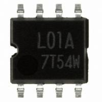
BR24L01AF-WE2 Rohm Semiconductor, BR24L01AF-WE2 Datasheet - Page 15

BR24L01AF-WE2
Manufacturer Part Number
BR24L01AF-WE2
Description
IC EEPROM 1KBIT 400KHZ 8SOP
Manufacturer
Rohm Semiconductor
Specifications of BR24L01AF-WE2
Memory Size
1K (128 x 8)
Format - Memory
EEPROMs - Serial
Memory Type
EEPROM
Speed
400kHz
Interface
I²C, 2-Wire Serial
Voltage - Supply
1.8 V ~ 5.5 V
Operating Temperature
-40°C ~ 85°C
Package / Case
8-SOP
Clock Frequency
400kHz
Supply Voltage Range
1.8V To 5.5V
Memory Case Style
SOP
No. Of Pins
8
Operating Temperature Range
-40°C To +85°C
Svhc
No SVHC (18-Jun-2010)
Package /
RoHS Compliant
Memory Configuration
128 X 8
Interface Type
I2C, Serial
Rohs Compliant
Yes
Lead Free Status / RoHS Status
Lead free / RoHS Compliant
Other names
BR24L01AF-WE2TR
Available stocks
Company
Part Number
Manufacturer
Quantity
Price
Company:
Part Number:
BR24L01AF-WE2
Manufacturer:
ROHM Semiconductor
Quantity:
1 835
Company:
Part Number:
BR24L01AF-WE2
Manufacturer:
ROHM
Quantity:
21 523
Part Number:
BR24L01AF-WE2
Manufacturer:
ROHM/罗姆
Quantity:
20 000
●WP valid timing (write cancel)
●Command cancel by start condition and stop condition
© 2009 ROHM Co., Ltd. All rights reserved.
BR24L□□-W Series,BR24S□□□-W Series
www.rohm.com
WP is usually fixed to 'H' or 'L', but when WP is used to cancel write cycle and so forth, pay attention to the following WP
valid timing. During write cycle execution, in cancel valid area, by setting WP='H', write cycle can be cancelled. In both byte
write cycle and page write cycle, the area from the first start condition of command to the rise of clock to taken in D0 of
data(in page write cycle, the first byte data) is cancel invalid area.
WP input in this area becomes Don't care. Set the setup time to rise of D0 taken SCL 100ns or more. The area from the rise
of SCL to take in D0 to the end of internal automatic write (tWR) is cancel valid area. And, when it is set WP='H' during tWR,
write is ended forcibly, data of address under access is not guaranteed, therefore, write it once again. (Refer to Fig.50.) After
execution of forced end by WP, standby status gets in, so there is no need to wait for tWR (5ms at maximum).
During command input, by continuously inputting start condition and stop condition, command can be cancelled.
(Refer to Fig. 51)
However, in ACK output area and during data read, SDA bus may output 'L', and in this case, start condition and stop
condition cannot be input, so reset is not available. Therefore, execute software reset. And when command is cancelled by
start, stop condition, during random read cycle, sequential read cycle, or current read cycle, internal setting address is not
determined, therefore, it is not possible to carry out current read cycle in succession. When to carry out read cycle in
succession, carry out random read cycle.
SDA
WP
SDA
SCL
S
T
A
R
T
SDA
SCL
Slave
address
・Rise of D0 taken clock
Fig.51 Case of cancel by start, stop condition during slave address input
A
C
K
L
Enlarged view
WP cancel invalid area
Word
address
D1
A
C
K
L
D0
1
D7 D6 D5 D4 D3 D2 D1 D0
ACK
0
Fig.50 WP valid timing
1
15/40
WP cancel valid area
A
C
K
L
Data is not written.
0
SCL
SDA
Data
Start condition
D0
Enlarged view
A
C
K
L
・Rise of SDA
ACK
O
S
T
P
Data not guaranteed
Write forced end
Stop condition
tWR
Technical Note
2009.09 - Rev.D


