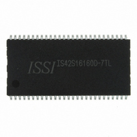
IS42S16160D-7TL ISSI, Integrated Silicon Solution Inc, IS42S16160D-7TL Datasheet - Page 27

IS42S16160D-7TL
Manufacturer Part Number
IS42S16160D-7TL
Description
IC SDRAM 256MBIT 143MHZ 54TSOP
Manufacturer
ISSI, Integrated Silicon Solution Inc
Type
SDRAMr
Specifications of IS42S16160D-7TL
Package / Case
54-TSOP II
Memory Size
256M (16Mx16)
Format - Memory
RAM
Memory Type
SDRAM
Speed
143MHz
Interface
Parallel
Voltage - Supply
3 V ~ 3.6 V
Operating Temperature
0°C ~ 70°C
Data Bus Width
16 bit
Maximum Clock Frequency
143 MHz
Access Time
6.5 ns, 5.4 ns
Supply Voltage (max)
3.6 V
Supply Voltage (min)
3 V
Maximum Operating Current
130 mA
Maximum Operating Temperature
+ 70 C
Minimum Operating Temperature
0 C
Mounting Style
SMD/SMT
Organization
16Mx16
Density
256Mb
Address Bus
15b
Access Time (max)
6.5/5.4ns
Maximum Clock Rate
143MHz
Operating Supply Voltage (typ)
3.3V
Package Type
TSOP-II
Operating Temp Range
0C to 70C
Operating Supply Voltage (max)
3.6V
Operating Supply Voltage (min)
3V
Supply Current
130mA
Pin Count
54
Mounting
Surface Mount
Operating Temperature Classification
Commercial
Lead Free Status / RoHS Status
Lead free / RoHS Compliant
Lead Free Status / RoHS Status
Lead free / RoHS Compliant, Lead free / RoHS Compliant
Other names
706-1074
IS42S16160D-7TL
IS42S16160D-7TL
Available stocks
Company
Part Number
Manufacturer
Quantity
Price
Company:
Part Number:
IS42S16160D-7TL
Manufacturer:
ISSI
Quantity:
1 000
Company:
Part Number:
IS42S16160D-7TL
Manufacturer:
ISSI
Quantity:
2
Part Number:
IS42S16160D-7TL
Manufacturer:
ISSI
Quantity:
20 000
Company:
Part Number:
IS42S16160D-7TLI
Manufacturer:
ISSI
Quantity:
1 000
Company:
Part Number:
IS42S16160D-7TLI
Manufacturer:
ISSI
Quantity:
2 770
IS42S83200D, IS42S16160D
CHIP OPERATION
BANK/ROW ACTIVATION
Before any READ or WRITE commands can be issued
to a bank within the SDRAM, a row in that bank must be
“opened.” This is accomplished via the ACTIVE command,
which selects both the bank and the row to be activated
(see Activating Specific Row Within Specific Bank).
After opening a row (issuing an ACTIVE command), a READ
or WRITE command may be issued to that row, subject to
the t
the clock period and rounded up to the next whole number
to determine the earliest clock edge after the ACTIVE
command on which a READ or WRITE command can be
entered. For example, a t
143 MHz clock (7ns period) results in 2.14 clocks, rounded
to 3. This is reflected in the following example, which cov-
ers any case where 2 < [t
procedure is used to convert other specification limits from
time units to clock cycles).
A subsequent ACTIVE command to a different row in the
same bank can only be issued after the previous active
row has been “closed” (precharged). The minimum time
interval between successive ACTIVE commands to the
same bank is defined by t
A subsequent ACTIVE command to another bank can be
issued while the first bank is being accessed, which results
in a reduction of total row-access overhead.The minimum
time interval between successive ACTIVE commands to
different banks is defined by t
EXAMPLE: MEETING TRCD (MIN) WHEN 2 < [TRCD (MIN)/TCK] ≤ 3
Integrated Silicon Solution, Inc. — www.issi.com
Rev. 00D
12/12/07
rcd
specification. Minimum t
COMMAND
rcd
rc
rcd
.
specification of 15ns with a
rrd
CLK
(MIN)/t
rcd
.
should be divided by
ck
ACTIVE
] ≤ 3. (The same
T0
t
NOP
RCD
T1
ACTIVATING SPECIFIC ROW WITHIN SPE-
CIFIC BANK
BA0, BA1
A0-A12
NOP
T2
CKE
RAS
CAS
CLK
WE
CS
HIGH
READ or
WRITE
T3
DON'T CARE
BANK ADDRESS
ROW ADDRESS
T4
27


