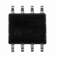
M45PE10-VMN6TP NUMONYX, M45PE10-VMN6TP Datasheet - Page 10

M45PE10-VMN6TP
Manufacturer Part Number
M45PE10-VMN6TP
Description
IC FLASH 1MBIT 75MHZ 8SOIC
Manufacturer
NUMONYX
Series
Forté™r
Datasheet
1.M45PE10-VMN6TP.pdf
(47 pages)
Specifications of M45PE10-VMN6TP
Format - Memory
FLASH
Memory Type
FLASH
Memory Size
1M (128K x 8)
Speed
75MHz
Interface
SPI, 3-Wire Serial
Voltage - Supply
2.7 V ~ 3.6 V
Operating Temperature
-40°C ~ 85°C
Package / Case
8-SOIC (3.9mm Width)
Lead Free Status / RoHS Status
Lead free / RoHS Compliant
Other names
M45PE10-VMN6TP
M45PE10-VMN6TPTR
M45PE10-VMN6TPTR
Available stocks
Company
Part Number
Manufacturer
Quantity
Price
Part Number:
M45PE10-VMN6TP
Manufacturer:
ST
Quantity:
20 000
SPI modes
3
10/47
SPI modes
These devices can be driven by a microcontroller with its SPI peripheral running in either of
the two following modes:
For these two modes, input data is latched in on the rising edge of Serial Clock (C), and
output data is available from the falling edge of Serial Clock (C).
The difference between the two modes, as shown in
bus master is in standby mode and not transferring data:
Figure 3.
1. The Write Protect (W) signal should be driven, High or Low as appropriate.
Figure 3
device is selected at a time, so only one device drives the serial data output (Q) line at a
time, the other devices are high impedance.
The pull-up resistor R (represented in
master leaves the S line in the high impedance state.
In applications where the bus master might enter a state where all inputs/outputs SPI lines
are in high impedance at the same time (for example, if the bus master is reset during the
transmission of an instruction), the Clock line (C) must be connected to an external pull-
down resistor so that, if all inputs/outputs become high impedance, the C line is pulled Low
(while the S line is pulled High). This ensures that S and C do not become High at the same
time, and so, that the t
SPI interface with
(CPOL, CPHA) =
CS3
(0, 0) or (1, 1)
SPI bus master
CPOL=0, CPHA=0
CPOL=1, CPHA=1
C remains at 0 for (CPOL=0, CPHA=0)
C remains at 1 for (CPOL=1, CPHA=1)
CS2 CS1
shows an example of three devices connected to an MCU, on an SPI bus. Only one
Bus master and memory devices on the SPI bus
SDO
SDI
SCK
R
SHCH
R
requirement is met.
C Q D
S
SPI memory
device
W
Figure
V
CC
Reset
V
R
3) ensures that no device is selected if the bus
SS
C Q D
S
Figure
SPI memory
device
W
4, is the clock polarity when the
V
Reset
CC
R
V
SS
C Q D
S
SPI memory
device
W
M45PE10
V
CC
Reset
AI12836c
V
SS
V
V
CC
SS


