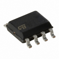
M95256-WMN6TP STMicroelectronics, M95256-WMN6TP Datasheet - Page 9

M95256-WMN6TP
Manufacturer Part Number
M95256-WMN6TP
Description
IC EEPROM 256KBIT 5MHZ 8SOIC
Manufacturer
STMicroelectronics
Specifications of M95256-WMN6TP
Format - Memory
EEPROMs - Serial
Memory Type
EEPROM
Memory Size
256K (32K x 8)
Speed
5MHz
Interface
SPI, 3-Wire Serial
Voltage - Supply
2.5 V ~ 5.5 V
Operating Temperature
-40°C ~ 85°C
Package / Case
8-SOIC (3.9mm Width)
Organization
32 K x 8
Interface Type
SPI
Maximum Clock Frequency
5 MHz
Access Time
60 ns
Supply Voltage (max)
6.5 V
Supply Voltage (min)
2.5 V
Maximum Operating Current
5 mA
Maximum Operating Temperature
+ 130 C
Mounting Style
SMD/SMT
Minimum Operating Temperature
- 40 C
Operating Supply Voltage
2.5 V, 5.5 V
Lead Free Status / RoHS Status
Lead free / RoHS Compliant
Other names
497-8691-2
M95256-WMN6TP
M95256-WMN6TP
Available stocks
Company
Part Number
Manufacturer
Quantity
Price
Company:
Part Number:
M95256-WMN6TP
Manufacturer:
STMicroelectronics
Quantity:
70 032
Part Number:
M95256-WMN6TP
Manufacturer:
ST
Quantity:
20 000
M95256-DR, M95256, M95256-W, M95256-R
3
3.1
3.2
3.3
3.4
3.5
Signal description
See
connected to this device.
Serial Data output (Q)
This output signal is used to transfer data serially out of the device. Data is shifted out on the
falling edge of Serial Clock (C).
Serial Data input (D)
This input signal is used to transfer data serially into the device. It receives instructions,
addresses, and the data to be written. Values are latched on the rising edge of Serial Clock
(C).
Serial Clock (C)
This input signal provides the timing of the serial interface. Instructions, addresses, or data
present at Serial Data input (D) are latched on the rising edge of Serial Clock (C). Data on
Serial Data output (Q) changes after the falling edge of Serial Clock (C).
Chip Select (S)
When this input signal is high, the device is deselected and Serial Data output (Q) is at high
impedance. Unless an internal Write cycle is in progress, the device will be in the Standby
Power mode. Driving Chip Select (S) low selects the device, placing it in the Active Power
mode.
After power-up, a falling edge on Chip Select (S) is required prior to the start of any
instruction.
Hold (HOLD)
The Hold (HOLD) signal is used to pause any serial communications with the device without
deselecting the device.
During the Hold condition, the Serial Data output (Q) is high impedance, and Serial Data
input (D) and Serial Clock (C) are Don’t Care.
To start the Hold condition, the device must be selected, with Chip Select (S) driven low.
Figure 1: Logic diagram
and
Doc ID 12276 Rev 13
Table 1: Signal
names, for a brief overview of the signals
Signal description
9/47


