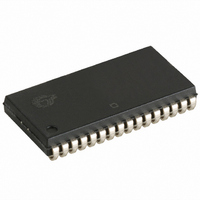
CY7C1018DV33-10VXI Cypress Semiconductor Corp, CY7C1018DV33-10VXI Datasheet - Page 6

CY7C1018DV33-10VXI
Manufacturer Part Number
CY7C1018DV33-10VXI
Description
IC SRAM 1MBIT 10NS 32SOJ
Manufacturer
Cypress Semiconductor Corp
Type
Asynchronousr
Datasheet
1.CY7C1018DV33-10VXI.pdf
(10 pages)
Specifications of CY7C1018DV33-10VXI
Memory Size
1M (128K x 8)
Package / Case
32-SOJ
Format - Memory
RAM
Memory Type
SRAM - Asynchronous
Speed
10ns
Interface
Parallel
Voltage - Supply
3 V ~ 3.6 V
Operating Temperature
-40°C ~ 85°C
Access Time
10 ns
Supply Voltage (max)
3.63 V
Supply Voltage (min)
2.97 V
Maximum Operating Current
60 mA
Maximum Operating Temperature
+ 85 C
Minimum Operating Temperature
- 40 C
Mounting Style
SMD/SMT
Number Of Ports
1
Operating Supply Voltage
3.3 V
Memory Configuration
128K X 8
Supply Voltage Range
3V To 3.6V
Memory Case Style
SOJ
No. Of Pins
32
Operating Temperature Range
-40°C To +85°C
Rohs Compliant
Yes
Lead Free Status / RoHS Status
Lead free / RoHS Compliant
Lead Free Status / RoHS Status
Lead free / RoHS Compliant, Lead free / RoHS Compliant
Other names
428-1963-5
CY7C1018DV33-10VXI
CY7C1018DV33-10VXI
Available stocks
Company
Part Number
Manufacturer
Quantity
Price
Part Number:
CY7C1018DV33-10VXI
Manufacturer:
CYPRESS/赛普拉斯
Quantity:
20 000
Document #: 38-05465 Rev. *E
Switching Waveforms
Write Cycle No. 1 (CE Controlled)
Write Cycle No. 2 (WE Controlled, OE HIGH During Write)
Notes
16. Data I/O is high impedance if OE = V
17. If CE goes HIGH simultaneously with WE going HIGH, the output remains in a high-impedance state.
18. During this period the I/Os are in the output state and input signals should not be applied.
ADDRESS
ADDRESS
DATA I/O
DATA I/O
WE
WE
CE
CE
OE
NOTE 18
(continued)
t
IH
SA
t
.
HZOE
[16, 17]
t
SA
t
AW
t
AW
t
SCE
t
t
WC
WC
[16, 17]
t
PWE
DATA
t
t
PWE
SD
DATA VALID
t
SCE
IN
t
t
SD
SCE
VALID
t
HD
t
HA
t
HA
t
HD
CY7C1018DV33
Page 6 of 10
[+] Feedback


