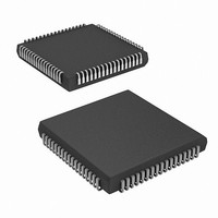
CY7C144-15JXI Cypress Semiconductor Corp, CY7C144-15JXI Datasheet - Page 11

CY7C144-15JXI
Manufacturer Part Number
CY7C144-15JXI
Description
IC SRAM 64KBIT 15NS 68PLCC
Manufacturer
Cypress Semiconductor Corp
Type
Asynchronousr
Datasheet
1.CY7C144-55AXC.pdf
(23 pages)
Specifications of CY7C144-15JXI
Memory Size
64K (8K x 8)
Package / Case
68-PLCC
Format - Memory
RAM
Memory Type
SRAM - Dual Port, Asynchronous
Speed
15ns
Interface
Parallel
Voltage - Supply
4.5 V ~ 5.5 V
Operating Temperature
-40°C ~ 85°C
Access Time
15 ns
Maximum Clock Frequency
1 MHz
Supply Voltage (max)
5.5 V
Supply Voltage (min)
4.5 V
Maximum Operating Current
220 mA
Organization
8 K x 8
Maximum Operating Temperature
+ 85 C
Minimum Operating Temperature
- 40 C
Mounting Style
SMD/SMT
Number Of Ports
2
Operating Supply Voltage
5 V
Lead Free Status / RoHS Status
Lead free / RoHS Compliant
Lead Free Status / RoHS Status
Lead free / RoHS Compliant, Lead free / RoHS Compliant
Available stocks
Company
Part Number
Manufacturer
Quantity
Price
Company:
Part Number:
CY7C144-15JXI
Manufacturer:
Cypress Semiconductor Corp
Quantity:
10 000
Switching Waveforms
Notes
Document #: 38-06034 Rev. *H
13. R/W is HIGH for read cycle.
14. Device is continuously selected CE = LOW and OE = LOW. This waveform cannot be used for semaphore reads.
15. Address valid prior to or coincident with CE transition LOW.
16. CE
17. BUSY = HIGH for the writing port.
18. CE
Data Out
Address
SEM or CE
Data Out
L
L
Address
Address
= L, SEM = H when accessing RAM. CE = H, SEM = L when accessing semaphores.
= CE
Data Out L
Data in
I
R
OE
I
CC
SB
R/W
= LOW.
R
R
R
L
Previous Data Valid
t
PU
t
OHA
Figure 6. Read Cycle No. 2 (Either Port CE/OE Access)
Figure 5. Read Cycle No. 1 (Either Port Address Access)
t
LZCE
Figure 7. Read Timing with Port-to-Port Delay (M/S=L)
t
LZOE
t
ACE
t
AA
t
DOE
Match
Match
t
WC
t
RC
t
PWE
t
WDD
Data Valid
t
Valid
SD
t
HZOE
[13, 15, 16]
t
Data Valid
DDD
[17, 18]
[13, 14]
t
HD
CY7C144 CY7C145
t
HZCE
t
PD
Valid
Page 11 of 23
[+] Feedback


