CY7C135-15JXC Cypress Semiconductor Corp, CY7C135-15JXC Datasheet - Page 3
CY7C135-15JXC
Manufacturer Part Number
CY7C135-15JXC
Description
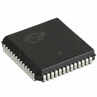
IC SRAM 32KBIT 15NS 52PLCC
Manufacturer
Cypress Semiconductor Corp
Type
Asynchronousr
Datasheet
1.CY7C135-15JXC.pdf
(12 pages)
Specifications of CY7C135-15JXC
Memory Size
32K (4K x 8)
Package / Case
52-PLCC
Format - Memory
RAM
Memory Type
SRAM - Dual Port, Asynchronous
Speed
15ns
Interface
Parallel
Voltage - Supply
4.5 V ~ 5.5 V
Operating Temperature
0°C ~ 70°C
Access Time
15 ns
Supply Voltage (max)
5.5 V
Supply Voltage (min)
4.5 V
Maximum Operating Current
220 mA
Maximum Operating Temperature
+ 70 C
Minimum Operating Temperature
0 C
Mounting Style
SMD/SMT
Number Of Ports
2
Operating Supply Voltage
5 V
Lead Free Status / RoHS Status
Lead free / RoHS Compliant
Lead Free Status / RoHS Status
Lead free / RoHS Compliant, Lead free / RoHS Compliant
Available stocks
Company
Part Number
Manufacturer
Quantity
Price
Company:

Part Number:
CY7C135-15JXC
Manufacturer:
Cypress Semiconductor Corp
Quantity:
10 000


Maximum Ratings
Exceeding maximum ratings may shorten the useful life of the
device. User guidelines are not tested.
Storage Temperature .................................. –65°C to+150°C
Ambient Temperature with
Power Applied ............................................. –55°C to+125°C
Supply Voltage to Ground Potential
(Pin 48 to Pin 24)............................................ –0.5V to+7.0V
DC Voltage Applied to Outputs
in High Z State ................................................ –0.5V to+7.0V
Electrical Characteristics
Document #: 38-06038 Rev. *D
V
V
V
V
I
I
I
I
I
I
I
IX
OZ
CC
SB1
SB2
SB3
SB4
Notes
Parameter
2. The voltage on any input or I/O pin cannot exceed the power pin during power up.
3. Pulse width < 20 ns.
4. f
OH
OL
IH
IL
I
MAX
SB3.
= 1/t
RC
= All inputs cycling at f = 1/t
Output HIGH Voltage
Output LOW Voltage
Input HIGH Voltage
Input LOW Voltage
Input Load Current
Output Leakage Current
Operating Current
Standby Current
(Both Ports TTL Levels)
Standby Current
(One Port TTL Level)
Standby Current
(Both Ports CMOS Levels)
Standby Current
(One Port CMOS Level)
Description
[2]
RC
Over the Operating Range
(except output enable). f = 0 means no address or control lines change. This applies only to inputs at CMOS level standby
V
V
GND ≤ V
Outputs Disabled,
GND ≤ V
V
I
CE
f = f
CE
f = f
Both Ports CE and CE
0.2V,
V
or V
One Port CE
CE
V
V
Active Port Outputs,
f = f
OUT
CC
CC
CC
IN
IN
IN
L
L
R
MAX
MAX
MAX
≥ V
≥V
≤ 0.2V,
IN
= Min., I
= Min., I
= Max.,
and CE
and CE
= 0 mA
≥ V
≤ 0.2V, f = 0
CC
CC
[4]
[4]
[4]
CC
I
O
– 0.2V or
≤ V
– 0.2V
≤ V
– 0.2V,
Test Conditions
R
R
L
OH
OL
CC
≥ V
≥ V
CC
or
= 4.0 mA
= –4.0 mA
IH
IH
[4]
,
,
R
≥ V
DC Input Voltage
Static Discharge Voltage........................................... > 2001V
(per MIL-STD-883, Method 3015)
Latch Up Current .................................................... > 200 mA
Operating Range
CC
Commercial
Industrial
–
Range
Com’l
Com’l
Com’l
Com’l
Com’l
Ind.
Ind.
Ind.
Ind.
Ind.
[3]
7C1342-15
Min
–10
–10
2.4
2.2
7C135-15
.........................................–3.0V to +7.0V
–40
Temperature
0
Max
+10
+10
220
130
125
0.4
0.8
60
15
°
Ambient
C to +70
°
C to +85
CY7C135, CY7C135A
7C1342-20
Min
–10
–10
7C135-20
2.4
2.2
°
C
°
C
Max
+10
+10
190
120
115
0.4
0.8
50
15
7C135A-25
7C1342-25 Unit
Min
–10
–10
2.4
2.2
7C135-25
CY7C1342
5V ± 10%
5V ± 10%
V
Page 3 of 12
Max
CC
+10
+10
180
190
110
120
100
115
0.4
0.8
40
50
15
30
mA
mA
mA
mA
mA
μA
μA
V
V
V
V
[+] Feedback
Related parts for CY7C135-15JXC
Image
Part Number
Description
Manufacturer
Datasheet
Request
R

Part Number:
Description:
Manufacturer:
Cypress Semiconductor Corp
Datasheet:
Part Number:
Description:
Manufacturer:
Cypress Semiconductor Corp
Datasheet:

Part Number:
Description:
CY7C135-25JXI
Manufacturer:
Cypress Semiconductor Corp
Datasheet:

Part Number:
Description:
IC SRAM 32KBIT 25NS 52PLCC
Manufacturer:
Cypress Semiconductor Corp
Datasheet:
Part Number:
Description:
Manufacturer:
Cypress Semiconductor Corp
Datasheet:
Part Number:
Description:
Manufacturer:
Cypress Semiconductor Corp
Datasheet:
Part Number:
Description:
Manufacturer:
Cypress Semiconductor Corp
Datasheet: