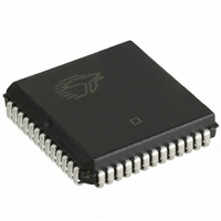
CY7C135-15JXC Cypress Semiconductor Corp, CY7C135-15JXC Datasheet - Page 4

CY7C135-15JXC
Manufacturer Part Number
CY7C135-15JXC
Description
IC SRAM 32KBIT 15NS 52PLCC
Manufacturer
Cypress Semiconductor Corp
Type
Asynchronousr
Datasheet
1.CY7C135-15JXC.pdf
(12 pages)
Specifications of CY7C135-15JXC
Memory Size
32K (4K x 8)
Package / Case
52-PLCC
Format - Memory
RAM
Memory Type
SRAM - Dual Port, Asynchronous
Speed
15ns
Interface
Parallel
Voltage - Supply
4.5 V ~ 5.5 V
Operating Temperature
0°C ~ 70°C
Access Time
15 ns
Supply Voltage (max)
5.5 V
Supply Voltage (min)
4.5 V
Maximum Operating Current
220 mA
Maximum Operating Temperature
+ 70 C
Minimum Operating Temperature
0 C
Mounting Style
SMD/SMT
Number Of Ports
2
Operating Supply Voltage
5 V
Lead Free Status / RoHS Status
Lead free / RoHS Compliant
Lead Free Status / RoHS Status
Lead free / RoHS Compliant, Lead free / RoHS Compliant
Available stocks
Company
Part Number
Manufacturer
Quantity
Price
Company:
Part Number:
CY7C135-15JXC
Manufacturer:
Cypress Semiconductor Corp
Quantity:
10 000
Electrical Characteristics
Capacitance
Note
Document #: 38-06038 Rev. *D
V
V
V
V
I
I
I
I
I
I
I
C
C
5. Tested initially and after any design or process changes that may affect these parameters.
IX
OZ
CC
SB1
SB2
SB3
SB4
Parameter
OH
OL
IH
IL
OUTPUT
IN
OUT
C = 30 pF
Parameter
(a) Normal Load (Load 1)
Output HIGH Voltage
Output LOW Voltage
Input LOW Voltage
Input Load Current
Output Leakage Current
Operating Current
Standby Current
(Both Ports TTL Levels)
Standby Current
(One Port TTL Level)
Standby Current
(Both Ports CMOS Levels)
Standby Current
(One Port CMOS Level)
[5]
Description
5V
Input Capacitance
Output Capacitance
R1 = 893Ω
R1 = 347Ω
Description
Over the Operating Range (continued)
Figure 3. AC Test Loads and Waveforms
GND
V
V
GND ≤ V
Outputs Disabled, GND ≤ V
V
V
CE
CE
Both Ports CE and CE
V
or V
One Port CE
V
Active Port Outputs, f = f
3.0V
CC
CC
CC
CC
IN
IN
L
L
≥ V
≥ V
≤ 3 ns
IN
= Min., I
= Min., I
= Max., I
= Max., I
and CE
and CE
OUTPUT
≤ 0.2V, f = 0
CC
CC
10%
I
C = 30 pF
≤ V
(b) Thévenin Equivalent (Load 1)
– 0.2V
– 0.2V or V
R
R
L
OH
OL
CC
OUT
OUT
≥ V
≥ V
or CE
T
V
Test Conditions
= 4.0 mA
ALL INPUT PULSES
= –4.0 mA
A
CC
90%
IH
IH
= 0 mA
= 0 mA
= 25°C, f = 1 MHz,
[4]
, f = f
, f = f
= 5.0V
R
R
IN
≥ V
R
TH
Test Conditions
≥ V
≤ 0.2V,
MAX
MAX
MAX
= 250Ω
CC
O
CC
[4]
[4]
[4]
– 0.2V,
≤ V
– 0.2V,
CC
90%
V
TH
10%
= 1.4V
≤ 3 ns
Com’l
Com’l
Com’l
Com’l
Com’l
Ind.
Ind.
Ind.
Ind.
Ind.
7C1342-35
Min
–10
–10
2.4
2.2
7C135-35
OUTPUT
(c) Three-State Delay (Load 3)
CY7C135, CY7C135A
Max.
10
10
C = 5 pF
Max
+10
+10
160
180
100
100
110
0.4
0.8
30
40
15
30
90
7C1342-55
Min
–10
–10
2.4
2.2
7C135-55
R
TH
CY7C1342
= 250Ω
Max
+10
+10
160
180
100
110
100
0.4
0.8
30
40
15
30
90
Unit
pF
pF
Page 4 of 12
Unit
mA
mA
mA
mA
mA
μA
μA
V
V
V
V
V
X
[+] Feedback


