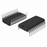
CAT28C16ALI90 ON Semiconductor, CAT28C16ALI90 Datasheet

IC EEPROM 16KBIT 90NS 24DIP

CAT28C16ALI90

Manufacturer Part Number
CAT28C16ALI90
Description
IC EEPROM 16KBIT 90NS 24DIP
Manufacturer
ON Semiconductor
Datasheet

Specifications of CAT28C16ALI90

Format - Memory
EEPROMs - Parallel
Memory Type
EEPROM
Memory Size
16K (2K x 8)
Speed
90ns
Interface
Parallel
Voltage - Supply
4.5 V ~ 5.5 V
Operating Temperature
-40°C ~ 85°C
Package / Case
24-DIP (0.600", 15.24mm)
Organization
2 K x 8
Interface Type
Parallel
Access Time
90 ns
Output Enable Access Time
50 ns
Supply Voltage (max)
5.5 V
Supply Voltage (min)
4.5 V
Maximum Operating Current
35 mA
Maximum Operating Temperature
+ 85 C
Mounting Style
Through Hole
Minimum Operating Temperature
- 40 C
Operating Supply Voltage
5 V
Lead Free Status / RoHS Status
Lead free / RoHS Compliant
Other names
28C16ALI-90
CAT28C16ALI-90
CAT28C16ALI-90
CAT28C16A
16 kb CMOS Parallel
EEPROM
Description
EEPROM organized as 2K x 8−bits. It requires a simple interface for
in−system programming. On−chip address and data latches,
self−timed write cycle with auto−clear and V
protection eliminate additional timing and protection hardware. DATA
Polling signals the start and end of the self−timed write cycle.
Additionally, the CAT28C16A features hardware write protection.
advanced CMOS floating gate technology. It is designed to endure
100,000 program/erase cycles and has a data retention of 100 years.
The device is available in JEDEC approved 24−pin DIP and SOIC or
32−pin PLCC packages.
Features
© Semiconductor Components Industries, LLC, 2009
October, 2009 − Rev. 6
I/O
I/O
I/O
V
The CAT28C16A is a fast, low power, 5V−only CMOS Parallel
The CAT28C16A is manufactured using ON Semiconductor’s
– Active: 25 mA Max.
– Standby: 100 mA Max.
– On−chip Address and Data Latches
– Self−timed Write Cycle with Auto−clear
SOIC Package (J, K, W, X)
A
A
A
A
A
A
A
A
SS
Fast Read Access Times: 90 ns, 120 ns, 200 ns
Low Power CMOS Dissipation:
Simple Write Operation:
Fast Write Cycle Time: 10 ms Max
End of Write Detection: DATA Polling
Hardware Write Protection
CMOS and TTL Compatible I/O
100,000 Program/Erase Cycles
100 Year Data Retention
Commercial, Industrial and Automotive Temperature Ranges
7
6
5
4
3
2
1
0
0
1
2
DIP Package (L)
2
3
4
5
6
7
8
9
10
11
12
1
24
23
22
21
20
19
18
17
16
15
14
13
PIN CONFIGURATION
V
A
A
WE
OE
A
CE
I/O
I/O
I/O
I/O
I/O
CC
8
9
10
7
6
5
4
3
I/O
NC
A
A
A
A
A
A
A
6
5
4
3
2
1
0
0
5
6
7
8
9
10
11
12
13
PLCC Package (N, G)
14 15 16 17 18 19 20
4 3 2 1 32 31 30
CC
TOP VIEW
power up/down write
29
28
27
26
25
24
23
22
21
1
A
A
NC
NC
OE
A
CE
I/O
I/O
8
9
10
7
6
See detailed ordering and shipping information in the package
dimensions section on page 10 of this data sheet.
Pin Name
I/O
A
CASE 646AD
0
V
V
WE
0
OE
CE
NC
−A
L SUFFIX
−I/O
CC
SS
PDIP−24
10
ORDERING INFORMATION
7
http://onsemi.com
J, K, W, X SUFFIX
PIN FUNCTION
CASE 751BK
Address Inputs
Data Inputs/Outputs
Chip Enable
Output Enable
Write Enable
5 V Supply
Ground
No Connect
SOIC−24
Publication Order Number:
Function
CASE 776AK
N, G SUFFIX
PLCC−32
CAT28C16A/D

Related parts for CAT28C16ALI90

CAT28C16ALI90 Summary of contents

Page 1

... DATA Polling signals the start and end of the self−timed write cycle. Additionally, the CAT28C16A features hardware write protection. The CAT28C16A is manufactured using ON Semiconductor’s advanced CMOS floating gate technology designed to endure 100,000 program/erase cycles and has a data retention of 100 years. ...

Page 2

ADDR. BUFFER A − & LATCHES INADVERTENT WRITE V CC PROTECTION CE CONTROL OE LOGIC WE TIMER ADDR. BUFFER A − & LATCHES Table 1. MODE SELECTION Mode Read Byte Write (WE Controlled) Byte Write (CE ...

Page 3

Table 4. RELIABILITY CHARACTERISTICS Symbol N (Note 5) Endurance END T (Notes 5) Data Retention DR V ESD Susceptibility ZAP I (Note 6) Latch−Up LTH 4. This parameter is tested initially and after a design or process change that affects ...

Page 4

V INPUT PULSE LEVELS 0.45 V Figure 2. A.C. Testing Input/Output Waveform 11. Input rise and fall times (10% and 90%) < 10 ns. Table 7. A.C. CHARACTERISTICS, WRITE CYCLE Symbol Parameter t Write Cycle Time WC t Address ...

Page 5

Read Data stored in the CAT28C16A is transferred to the data bus when WE is held high, and both OE and CE are held low. The data bus is set to a high impedance state when either ...

Page 6

DATA Polling DATA polling is provided to indicate the completion of a byte write cycle. Once a byte write cycle is initiated, attempting to read the last byte written will output the ADDRESS OES t ...

Page 7

PIN#1 IDENTIFICATION D1 D TOP VIEW SIDE VIEW Notes: (1) All dimensions are in millimeters. (2) Complies with JEDEC MS-016. PACKAGE DIMENSIONS PLCC 32 CASE 776AK−01 ISSUE SYMBOL ...

Page 8

PIN#1 IDENTIFICATION TOP VIEW D A SIDE VIEW Notes: (1) All dimensions are in millimeters. Angles in degrees. (2) Complies with JEDEC MS-013. PACKAGE DIMENSIONS SOIC−24, 300 mils CASE 751BK−01 ISSUE O SYMBOL ...

Page 9

D TOP VIEW b1 e SIDE VIEW Notes: (1) All dimensions are in millimeters. (2) Complies with JEDEC MS-011. PACKAGE DIMENSIONS PDIP−24, 600 mils CASE 646AD−01 ISSUE A SYMBOL ...

Page 10

... Opportunity/Affirmative Action Employer. This literature is subject to all applicable copyright laws and is not for resale in any manner. PUBLICATION ORDERING INFORMATION LITERATURE FULFILLMENT: Literature Distribution Center for ON Semiconductor P.O. Box 5163, Denver, Colorado 80217 USA Phone: 303−675−2175 or 800−344−3860 Toll Free USA/Canada Fax: 303− ...

Related keywords