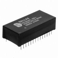
DS1244Y-70+ Maxim Integrated Products, DS1244Y-70+ Datasheet - Page 5

DS1244Y-70+
Manufacturer Part Number
DS1244Y-70+
Description
IC NVSRAM 256KBIT 70NS 28DIP
Manufacturer
Maxim Integrated Products
Datasheet
1.DS1244Y-70.pdf
(19 pages)
Specifications of DS1244Y-70+
Format - Memory
RAM
Memory Type
NVSRAM (Non-Volatile SRAM)
Memory Size
256K (32K x 8)
Speed
70ns
Interface
Parallel
Voltage - Supply
4.5 V ~ 5.5 V
Operating Temperature
0°C ~ 70°C
Package / Case
28-DIP Module (600 mil), 28-EDIP
Organization
32 K x 8
Supply Voltage (max)
5.5 V
Supply Voltage (min)
4.5 V
Operating Current
85 mA
Maximum Operating Temperature
+ 70 C
Minimum Operating Temperature
0 C
Mounting Style
SMD/SMT
Lead Free Status / RoHS Status
Lead free / RoHS Compliant
DATA RETENTION MODE
The 5V device is fully accessible and data can be written or read only when V
However, when V
internal clock registers and SRAM are blocked from any access. When V
point, V
operation and SRAM data are maintained from the battery until V
The 3.3V device is fully accessible and data can be written or read only when V
When V
power is switched from V
than V
V
levels.
All control, data, and address signals must be powered down when V
PHANTOM CLOCK OPERATION
Communication with the phantom clock is established by pattern recognition on a serial bit stream of
64 bits, which must be matched by executing 64 consecutive write cycles containing the proper data on
DQ0. All accesses that occur prior to recognition of the 64-bit pattern are directed to memory.
After recognition is established, the next 64 read or write cycles either extract or update data in the
phantom clock, and memory access is inhibited.
Data transfer to and from the timekeeping function is accomplished with a serial bit stream under control
of the chip enable, output enable, and write enable. Initially, a read cycle to any memory location using
the
to the first bit of the 64-bit comparison register. Next, 64 consecutive write cycles are executed using the
phantom clock. Therefore, any address to the memory in the socket is acceptable. However, the write
cycles generated to gain access to the phantom clock are also writing data to a location in the mated
RAM. The preferred way to manage this requirement is to set aside just one address location in RAM as a
phantom clock scratch pad. When the first write cycle is executed, it is compared to bit 0 of the 64-bit
comparison register. If a match is found, the pointer increments to the next location of the comparison
register and awaits the next write cycle. If a match is not found, the pointer does not advance and all
subsequent write cycles are ignored. If a read cycle occurs at any time during pattern recognition, the
present sequence is aborted and the comparison register pointer is reset. Pattern recognition continues for
a total of 64 write cycles as described above until all the bits in the comparison register have been
matched (Figure 1). With a correct match for 64 bits, the phantom clock is enabled and data transfer to or
from the timekeeping registers can proceed. The next 64 cycles will cause the phantom clock to either
receive or transmit data on DQ0, depending on the level of the
locations outside the memory block can be interleaved with
recognition sequence or data transfer sequence to the phantom clock.
CE
BAT
CE
and
. RTC operation and SRAM data are maintained from the battery until V
BAT
and
SO
CC
WE
, the device power is switched from V
(battery supply level), device power is switched from the V
fall as below the V
OE
control of the SmartWatch. These 64 write cycles are used only to gain access to the
control of the phantom clock starts the pattern recognition sequence by moving a pointer
CC
is below the power fail point, V
CC
to the backup supply (V
PF
, access to the device is inhibited. If V
CC
to the backup supply (V
5 of 19
BAT
PF
) when V
(point at which write protection occurs), the
CE
CC
OE
cycles without interrupting the pattern
CC
is returned to nominal levels.
CC
pin or the
drops below V
CC
is powered down.
CC
PF
pin to the backup battery. RTC
falls below the battery switch
is less than V
BAT
CC
) when V
WE
CC
CC
is returned to nominal
pin. Cycles to other
is greater than V
is greater than V
PF
. If V
CC
BAT
drops below
, the device
PF
is greater
PF
PF
.
.


