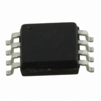
W25X40BVSSIG Winbond Electronics, W25X40BVSSIG Datasheet - Page 16

W25X40BVSSIG
Manufacturer Part Number
W25X40BVSSIG
Description
IC SPI FLASH 4MBIT 8SOIC
Manufacturer
Winbond Electronics
Datasheet
1.W25X40BVSNIG.pdf
(51 pages)
Specifications of W25X40BVSSIG
Format - Memory
FLASH
Memory Type
FLASH
Memory Size
4M (512K x 8)
Speed
104MHz
Interface
SPI Serial
Voltage - Supply
2.7 V ~ 3.6 V
Operating Temperature
-40°C ~ 85°C
Package / Case
8-SOIC (5.3mm Width), 8-SOP, 8-SOEIAJ
Lead Free Status / RoHS Status
Lead free / RoHS Compliant
Available stocks
Company
Part Number
Manufacturer
Quantity
Price
Company:
Part Number:
W25X40BVSSIG
Manufacturer:
WINBOND
Quantity:
6 000
Company:
Part Number:
W25X40BVSSIG
Manufacturer:
WINBOND
Quantity:
20 186
Part Number:
W25X40BVSSIG
Manufacturer:
WINBOND/华邦
Quantity:
20 000
9.2.3
The Write Enable instruction (Figure 4) sets the Write Enable Latch (WEL) bit in the Status Register to
a 1. The WEL bit must be set prior to every Page Program, Sector Erase, Block Erase, Chip Erase
and Write Status Register instruction. The Write Enable instruction is entered by driving /CS low,
shifting the instruction code “06h” into the Data Input (DI) pin on the rising edge of CLK, and then
driving /CS high.
9.2.4
The Write Disable instruction (Figure 5) resets the Write Enable Latch (WEL) bit in the Status Register
to a 0. The Write Disable instruction is entered by driving /CS low, shifting the instruction code “04h”
into the DIO pin and then driving /CS high. Note that the WEL bit is automatically reset after Power-up
and upon completion of the Write Status Register, Page Program, Sector Erase, Block Erase and
Chip Erase instructions.
Write Enable (06h)
Write Disable (04h)
Figure 5. Write Disable Instruction Sequence Diagram
Figure 4. Write Enable Instruction Sequence Diagram
- 16 -
W25X10BV/20BV/40BV


