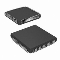
CY7C138-25JXI Cypress Semiconductor Corp, CY7C138-25JXI Datasheet - Page 5

CY7C138-25JXI
Manufacturer Part Number
CY7C138-25JXI
Description
IC SRAM 32KBIT 25NS 68PLCC
Manufacturer
Cypress Semiconductor Corp
Type
Asynchronousr
Datasheet
1.CY7C138-25JXC.pdf
(21 pages)
Specifications of CY7C138-25JXI
Memory Size
32K (4K x 8)
Package / Case
68-PLCC
Format - Memory
RAM
Memory Type
SRAM - Dual Port, Asynchronous
Speed
25ns
Interface
Parallel
Voltage - Supply
4.5 V ~ 5.5 V
Operating Temperature
-40°C ~ 85°C
Access Time
25 ns
Maximum Clock Frequency
1 MHz
Supply Voltage (max)
5.5 V
Supply Voltage (min)
4.5 V
Maximum Operating Current
180 mA
Organization
4 K x 8
Maximum Operating Temperature
+ 85 C
Minimum Operating Temperature
- 40 C
Mounting Style
SMD/SMT
Number Of Ports
2
Operating Supply Voltage
5 V
Lead Free Status / RoHS Status
Lead free / RoHS Compliant
Lead Free Status / RoHS Status
Lead free / RoHS Compliant, Lead free / RoHS Compliant
Available stocks
Company
Part Number
Manufacturer
Quantity
Price
Company:
Part Number:
CY7C138-25JXI
Manufacturer:
Cypress Semiconductor
Quantity:
135
Company:
Part Number:
CY7C138-25JXI
Manufacturer:
Cypress Semiconductor Corp
Quantity:
10 000
Capacitance
Switching Characteristics
Document #: 38-06037 Rev. *G
t
t
t
t
t
t
t
t
t
t
t
t
t
Notes
C
C
RC
AA
OHA
ACE
DOE
LZOE
HZOE
LZCE
HZCE
PU
PD
WC
SCE
6. Tested initially and after any design or process changes that may affect these parameters.
7. Test conditions assume signal transition time of 3 ns or less, timing reference levels of 1.5 V, input pulse levels of 0 to 3.0 V, and output loading of the specified I
8. At any temperature and voltage condition for any device, t
9. Test conditions used are Load 3
10. This parameter is guaranteed but not tested.
READ CYCLE
WRITE CYCLE
IN
OUT
Output
[10]
[10]
and 30-pF load capacitance.
Output
[8,9,10]
[8,9,10]
[8,9,10]
[8,9,10]
C = 30 pF
Parameter
Parameter
(a) Normal Load (Load 1)
Load (Load 2)
[6]
C = 30 pF
Read cycle time
Address to data valid
Output hold from address change
CE LOW to data valid
OE LOW to data valid
OE Low to Low Z
OE HIGH to High Z
CE LOW to Low Z
CE HIGH to High Z
CE LOW to Power-up
CE HIGH to Power-down
Write cycle time
CE LOW to write end
5 V
Input capacitance
Output capacitance
R1 = 893
R2 = 347
Description
Over the Operating Range
GND
3.0 V
Figure 2. AC Test Loads and Waveforms
< 3 ns
Output
HZCE
10%
Description
C = 30pF
(b) Thé venin Equivalent ( Load 1)
is less than t
All Input Pulses
90%
T
V
A
CC
= 25 C, f = 1 MHz,
LZCE
R
[7]
= 5.0 V
TH
and t
= 250
Test Conditions
HZOE
is less than t
V
90%
TH
10%
= 1.4 V
< 3 ns
LZOE
.
Output
Min
C = 5 pF
25
25
20
–
3
–
–
3
–
3
–
0
–
(c) Three-State Delay (Load 3)
7C138-25
Max
10
15
Max
25
25
15
15
15
25
–
–
–
–
–
–
–
5V
CY7C138
R1 = 893
R2 = 347
Page 5 of 21
Unit
pF
pF
Unit
ns
ns
ns
ns
ns
ns
ns
ns
ns
ns
ns
ns
ns
OI
/I
OH
[+] Feedback


