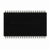
MR0A08BYS35 EverSpin Technologies Inc, MR0A08BYS35 Datasheet - Page 5

MR0A08BYS35
Manufacturer Part Number
MR0A08BYS35
Description
IC MRAM 1MBIT 35NS 44TSOP
Manufacturer
EverSpin Technologies Inc
Datasheet
1.MR0A08BYS35.pdf
(15 pages)
Specifications of MR0A08BYS35
Format - Memory
RAM
Memory Type
MRAM (Magnetoresistive RAM)
Memory Size
1M (128K x 8)
Speed
35ns
Interface
Parallel
Voltage - Supply
3 V ~ 3.6 V
Operating Temperature
0°C ~ 70°C
Package / Case
44-TSOP II
Word Size
8b
Organization
128Kx8
Density
1Mb
Interface Type
Parallel
Access Time (max)
35ns
Operating Supply Voltage (typ)
3.3V
Operating Temperature Classification
Commercial
Operating Supply Voltage (max)
3.6V
Operating Supply Voltage (min)
3V
Operating Temp Range
0C to 70C
Pin Count
44
Mounting
Surface Mount
Supply Current
65mA
Lead Free Status / RoHS Status
Lead free / RoHS Compliant
Lead Free Status / RoHS Status
Compliant, Lead free / RoHS Compliant
Other names
819-1002
Available stocks
Company
Part Number
Manufacturer
Quantity
Price
Part Number:
MR0A08BYS35R
Manufacturer:
EVERSPIN
Quantity:
20 000
Everspin Technologies © 2009
Electrical Specifications
Power Up and Power Down Sequencing
MRAM is protected from write operations whenever V
there is a startup time of 2 ms before read or write operations can start. This time allows memory power
supplies to stabilize.
The E and W control signals should track V
high for the startup time. In most systems, this means that these signals should be pulled up with a resis-
tor so that signal remains high if the driving signal is Hi-Z during power up. Any logic that drives E and W
should hold the signals high with a power-on reset signal for longer than the startup time.
During power loss or brownout where V
observed when power returns above V
i
ii
iii
iv
V
Automotive temperature profile assumes 10% duty cycle at maximum temperature (2-years out of 20-year life)
Parameter
Power supply voltage
Write inhibit voltage
Input high voltage
Input low voltage
Temperature under bias
There is a 2 ms startup time once V
V
MR0A08B (Commercial)
MR0A08BC (Industrial)
MR0A08BM (Automotive)
IH
IL
(min) = -0.5 V
(max) = V
WRITES INHIBITED
DD
+ 0.3 V
DC
; V
V
W
E
WI
IL
DC
(min) = -2.0 V
; V
IH
(max) = V
Figure 2.1 Power Up and Power Down Diagram
iv
STARTUP TIME
AC
DD
(pulse width ≤ 10 ns) for I ≤ 20.0 mA.
exceeds V
DD
+ 2.0 V
NORMAL OPERATION
Table 2.2 Operating Conditions
DD
Symbol
V
V
V
V
T
A
DD
DD
WI
IH
IL
(min).
AC
DD,
goes below V
V
DD
(pulse width ≤ 10 ns) for I ≤ 20.0 mA.
DD
(max). See Power Up and Power Down Sequencing below.
on power up to V
BROWNOUT OR POWER LOSS
Value
3.0
2.5
2.2
-0.5
0
-40
-40
5
DD
i
iii
is less than V
WI
, writes are protected and a startup time must be
STARTUP TIME
Document Number: MR0A08B Rev. 2, 6/2009
DD
- 0.2 V or V
NORMAL OPERATION
WI
. As soon as V
Typical
3.3
2.7
-
-
V
DD
IH
(whichever is lower) and remain
V
WI
DD
Max
3.6
3.0
V
0.8
70
85
125
MR0A08B
exceeds V
DD
i
+ 0.3
ii
DD
Unit
V
V
V
V
°C
(min),


