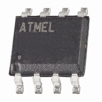
AT25DF041A-SH-T Atmel, AT25DF041A-SH-T Datasheet - Page 13

AT25DF041A-SH-T
Manufacturer Part Number
AT25DF041A-SH-T
Description
IC FLASH 4MBIT 70MHZ 8SOIC
Manufacturer
Atmel
Datasheet
1.AT25DF041A-MHF-Y.pdf
(41 pages)
Specifications of AT25DF041A-SH-T
Format - Memory
FLASH
Memory Type
DataFLASH
Memory Size
4M (2048 pages x 256 bytes)
Speed
70MHz
Interface
SPI, 3-Wire Serial
Voltage - Supply
2.7 V ~ 3.6 V
Operating Temperature
-40°C ~ 85°C
Package / Case
8-SOIC (3.9mm Width)
Lead Free Status / RoHS Status
Lead free / RoHS Compliant
Available stocks
Company
Part Number
Manufacturer
Quantity
Price
Company:
Part Number:
AT25DF041A-SH-T
Manufacturer:
NANYA
Quantity:
3 000
Part Number:
AT25DF041A-SH-T
Manufacturer:
ATMEL/爱特梅尔
Quantity:
20 000
3668D–DFLASH–9/08
If the address specified by A23 - A0 points to a memory location within a sector that is in the pro-
tected state, then the Block Erase command will not be executed, and the device will return to
the idle state once the CS pin has been deasserted. In addition, with the larger Block Erase
sizes of 32K and 64 Kbytes, more than one physical sector may be erased (e.g. sectors 18
through 15) at one time. Therefore, in order to erase a larger block that may span more than one
sector, all of the sectors in the span must be in the unprotected state. If one of the physical sec-
tors within the span is in the protected state, then the device will ignore the Block Erase
command and will return to the idle state once the CS pin is deasserted.
The WEL bit in the Status Register will be reset back to the logical “0” state if the erase cycle
aborts due to an incomplete address being sent or because a memory location within the region
to be erased is protected.
While the device is executing a successful erase cycle, the Status Register can be read and will
indicate that the device is busy. For faster throughput, it is recommended that the Status Regis-
ter be polled rather than waiting the t
some point before the erase cycle completes, the WEL bit in the Status Register will be reset
back to the logical “0” state.
The device also incorporates an intelligent erase algorithm that can detect when a byte location
fails to erase properly. If an erase error occurs, it will be indicated by the EPE bit in the Status
Register.
Figure 8-5.
SCK
CS
SO
SI
Block Erase
HIGH-IMPEDANCE
MSB
C
0
C
1
C
2
OPCODE
C
3
C
4
BLKE
C
5
C
6
time to determine if the device has finished erasing. At
C
7
MSB
A
8
A
9
A
10 11
A
ADDRESS BITS A23-A0
A
12
A
A
26
A
27 28
A
AT25DF041A
A
29 30
A
A
31
13


