AT25DF021-MH-Y Atmel, AT25DF021-MH-Y Datasheet - Page 21
AT25DF021-MH-Y
Manufacturer Part Number
AT25DF021-MH-Y
Description
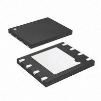
IC FLASH 2MBIT 70MHZ 8UDFN
Manufacturer
Atmel
Datasheet
1.AT25DF021-SSH-B.pdf
(41 pages)
Specifications of AT25DF021-MH-Y
Format - Memory
FLASH
Memory Type
DataFLASH
Memory Size
2M (256K x 8)
Speed
70MHz
Interface
SPI, 3-Wire Serial
Voltage - Supply
2.7 V ~ 3.6 V
Operating Temperature
-40°C ~ 85°C
Package / Case
8-UDFN
Lead Free Status / RoHS Status
Lead free / RoHS Compliant


Figure 10-1. Program OTP Security Register
10.2
Figure 10-2. Read OTP Security Register
3677D–DFLASH–04/09
SCK
SO
CS
SI
SCK
SO
CS
Read OTP Security Register
SI
MSB
HIGH-IMPEDANCE
0
0
1
1
MSB
HIGH-IMPEDANCE
1
1
2
OPCODE
0
1
0
3
1
0
The OTP Security Register can be sequentially read in a similar fashion to the Read Array oper-
ation up to the maximum clock frequency specified by f
the CS pin must first be asserted and the opcode of 77h must be clocked into the device. After
the opcode has been clocked in, the three address bytes must be clocked in to specify the start-
ing address location of the first byte to read within the OTP Security Register. Following the
three address bytes, two dummy bytes must be clocked into the device before data can be
output.
After the three address bytes and the dummy bytes have been clocked in, additional clock
cycles will result in OTP Security Register data being output on the SO pin. When the last byte
(00007Fh) of the OTP Security Register has been read, the device will continue reading back at
the beginning of the register (000000h). No delays will be incurred when wrapping around from
the end of the register to the beginning of the register.
Deasserting the CS pin will terminate the read operation and put the SO pin into a high-imped-
ance state. The CS pin can be deasserted at any time and does not require that a full byte of
data be read.
0
4
2
OPCODE
1
1
5
3
1
1
6
4
1
0
7
5
MSB
A
1
8
6
A
1
9
7
ADDRESS BITS A23-A0
MSB
A
10 11
A
ADDRESS BITS A23-A0
8
A
A
9
A
12
A
A
A
29 30
A
29 30
A
A
A
31 32
MSB
A
31 32
D
MSB
X
D
33
DATA IN BYTE 1
X
33
D
34
X
34
D
35
X
DON'T CARE
35
D
36
X
36
D
37 38
X
D
D
39
CLK
X
. To read the OTP Security Register,
X
MSB
D
X
MSB
D
D
DATA IN BYTE n
D
D
DATA BYTE 1
D
D
D
D
D
D
D
D
D
D
D
MSB
D
D
21
Related parts for AT25DF021-MH-Y
Image
Part Number
Description
Manufacturer
Datasheet
Request
R

Part Number:
Description:
One mechanical button switch Three LEDs Four expansion headers
Manufacturer:
ATMEL [ATMEL Corporation]
Datasheet:

Part Number:
Description:
IC FLASH 2MBIT 70MHZ 8SOIC
Manufacturer:
Atmel
Datasheet:
Part Number:
Description:
IC FLASH 2MBIT 70MHZ 8SOIC
Manufacturer:
Atmel
Datasheet:
Part Number:
Description:
IC FLASH 2MBIT 70MHZ 8SOIC
Manufacturer:
Atmel
Datasheet:
Part Number:
Description:
IC FLASH 2MBIT 70MHZ 8SOIC
Manufacturer:
Atmel
Datasheet:

Part Number:
Description:
IC FLASH 2MBIT 70MHZ 8UDFN
Manufacturer:
Atmel
Datasheet:
Part Number:
Description:
IC FLASH 2MBIT 70MHZ 8UDFN
Manufacturer:
Atmel
Datasheet:
Part Number:
Description:
IC FLASH 2MBIT 70MHZ 8UDFN
Manufacturer:
Atmel
Datasheet:

Part Number:
Description:
2-megabit 2.3-volt Or 2.7-volt Minimum Spi Serial Flash Memory
Manufacturer:
ATMEL Corporation
Datasheet:


Part Number:
Description:
DEV KIT FOR AVR/AVR32
Manufacturer:
Atmel
Datasheet:
Part Number:
Description:
INTERVAL AND WIPE/WASH WIPER CONTROL IC WITH DELAY
Manufacturer:
ATMEL Corporation
Datasheet: