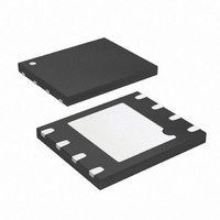
AT25DF081-MHN-Y Atmel, AT25DF081-MHN-Y Datasheet - Page 23

AT25DF081-MHN-Y
Manufacturer Part Number
AT25DF081-MHN-Y
Description
IC FLASH 8MBIT 66MHZ 8UDFN
Manufacturer
Atmel
Datasheet
1.AT25DF081-SSHN-T.pdf
(38 pages)
Specifications of AT25DF081-MHN-Y
Format - Memory
FLASH
Memory Type
DataFLASH
Memory Size
8M (4096 pages x 256 bytes)
Speed
66MHz
Interface
SPI, 3-Wire Serial
Voltage - Supply
1.65 V ~ 1.95 V
Operating Temperature
-40°C ~ 85°C
Package / Case
8-UDFN
Lead Free Status / RoHS Status
Lead free / RoHS Compliant
11. Other Commands and Functions
11.1
3674E–DFLASH–8/08
Read Manufacturer and Device ID
The complete one byte of data must be clocked into the device before the CS pin is deasserted,
and the CS pin must be deasserted on an even byte boundary (multiples of eight bits); other-
wise, the device will abort the operation, the state of the SPRL bit will not change, no potential
Global Protect or Unprotect will be performed, and the WEL bit in the Status Register will be
reset back to the logical “0” state.
If the WP pin is asserted, then the SPRL bit can only be set to a logical “1”. If an attempt is made
to reset the SPRL bit to a logical “0” while the WP pin is asserted, then the Write Status Register
command will be ignored, and the WEL bit in the Status Register will be reset back to the logical
“0” state. In order to reset the SPRL bit to a logical “0”, the WP pin must be deasserted.
Table 10-2.
Figure 10-2. Write Status Register
Identification information can be read from the device to enable systems to electronically query
and identify the device while it is in system. The identification method and the command opcode
comply with the JEDEC standard for “Manufacturer and Device ID Read Methodology for SPI
Compatible Serial Interface Memory Devices”. The type of information that can be read from the
device includes the JEDEC defined Manufacturer ID, the vendor specific Device ID, and the ven-
dor specific Extended Device Information.
To read the identification information, the CS pin must first be asserted and the opcode of 9Fh
must be clocked into the device. After the opcode has been clocked in, the device will begin out-
putting the identification data on the SO pin during the subsequent clock cycles. The first byte
that will be output will be the Manufacturer ID followed by two bytes of Device ID information.
The fourth byte output will be the Extended Device Information String Length, which will be 00h
indicating that no Extended Device Information follows. After the Extended Device Information
String Length byte is output, the SO pin will go into a high-impedance state; therefore, additional
clock cycles will have no affect on the SO pin and no data will be output. As indicated in the
JEDEC standard, reading the Extended Device Information String Length and any subsequent
data is optional.
SPRL
Bit 7
Write Status Register Format
SCK
SO
CS
Bit 6
SI
X
Bit 5
HIGH-IMPEDANCE
MSB
0
0
0
1
0
2
OPCODE
Global Protect/Unprotect
0
3
Bit 4
0
4
0
5
0
6
1
7
MSB
D
8
Bit 3
STATUS REGISTER IN
X
9
D
10 11
D
D
12
Bit 2
D
13
X
14 15
X
AT25DF081
Bit 1
X
Bit 0
X
23


