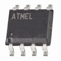
AT25DF161-SH-T Atmel, AT25DF161-SH-T Datasheet - Page 10

AT25DF161-SH-T
Manufacturer Part Number
AT25DF161-SH-T
Description
IC FLASH 16MBIT 100MHZ 8SOIC
Manufacturer
Atmel
Datasheet
1.AT25DF161-SH-B.pdf
(52 pages)
Specifications of AT25DF161-SH-T
Format - Memory
FLASH
Memory Type
DataFLASH
Memory Size
16M (2M x 8)
Speed
100MHz
Interface
SPI, RapidS
Voltage - Supply
2.7 V ~ 3.6 V
Operating Temperature
-40°C ~ 85°C
Package / Case
8-SOIC (5.3mm Width), 8-SOP, 8-SOEIAJ
Density
16Mb
Access Time (max)
5ns
Interface Type
Serial (SPI)
Boot Type
Not Required
Address Bus
1b
Operating Supply Voltage (typ)
3.3V
Operating Temp Range
-40C to 85C
Package Type
SOIC EIAJ
Program/erase Volt (typ)
2.7 to 3.6V
Sync/async
Synchronous
Operating Temperature Classification
Industrial
Operating Supply Voltage (min)
2.7V
Operating Supply Voltage (max)
3.6V
Word Size
8b
Number Of Words
2M
Supply Current
19mA
Mounting
Surface Mount
Pin Count
8
Lead Free Status / RoHS Status
Lead free / RoHS Compliant
Available stocks
Company
Part Number
Manufacturer
Quantity
Price
8.
8.1
10
Deasserting the CS pin will terminate the read operation and put the SO and SIO pins into a high-impedance state. The CS
pin can be deasserted at any time and does not require that a full byte of data be read.
Figure 7-4.
Program and Erase Commands
Byte/Page Program
The Byte/Page Program command allows anywhere from a single byte of data to 256-bytes of data to be programmed
into previously erased memory locations. An erased memory location is one that has all eight bits set to the logical “1”
state (a byte value of FFh). Before a Byte/Page Program command can be started, the Write Enable command must have
been previously issued to the device (see
Status Register to a logical “1” state.
To perform a Byte/Page Program command, an opcode of 02h must be clocked into the device followed by the three
address bytes denoting the first byte location of the memory array to begin programming at. After the address bytes have
been clocked in, data can then be clocked into the device and will be stored in an internal buffer.
If the starting memory address denoted by A23-A0 does not fall on an even 256-byte page boundary (A7-A0 are not all
0), then special circumstances regarding which memory locations to be programmed will apply. In this situation, any data
that is sent to the device that goes beyond the end of the page will wrap around back to the beginning of the same page.
For example, if the starting address denoted by A23-A0 is 0000FEh, and three bytes of data are sent to the device, then
the first two bytes of data will be programmed at addresses 0000FEh and 0000FFh while the last byte of data will be
programmed at address 000000h. The remaining bytes in the page (addresses 000001h through 0000FDh) will not be
programmed and will remain in the erased state (FFh). In addition, if more than 256-bytes of data are sent to the device,
then only the last 256-bytes sent will be latched into the internal buffer.
When the CS pin is deasserted, the device will take the data stored in the internal buffer and program it into the
appropriate memory array locations based on the starting address specified by A23-A0 and the number of data bytes sent
to the device. If less than 256 bytes of data were sent to the device, then the remaining bytes within the page will not be
programmed and will remain in the erased state (FFh). The programming of the data bytes is internally self-timed and
should take place in a time of t
The three address bytes and at least one complete byte of data must be clocked into the device before the CS pin is
deasserted, and the CS pin must be deasserted on even byte boundaries (multiples of eight bits); otherwise, the device
will abort the operation and no data will be programmed into the memory array. In addition, if the address specified by
A23-A0 points to a memory location within a sector that is in the protected state (see
locked down (see
Atmel AT25DF161
SCK
SIO
SO
CS
Dual-Output Read Array
“Sector Lockdown” on page
PP
or t
BP
if only programming a single byte.
“Write Enable” on page
25), then the Byte/Page Program command will not be executed, and
18) to set the Write Enable Latch (WEL) bit of the
“Protect Sector” on page
3687E–DFLASH–11/10
19) or


