AT28C010-15UM/883 Atmel, AT28C010-15UM/883 Datasheet - Page 3
AT28C010-15UM/883
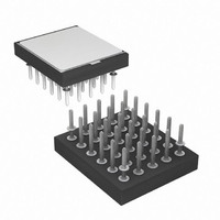
Manufacturer Part Number
AT28C010-15UM/883
Description
IC EEPROM 1MBIT 150NS 30PGA
Manufacturer
Atmel
Datasheet
1.AT28C010-15EM883.pdf
(17 pages)
Specifications of AT28C010-15UM/883
Format - Memory
EEPROMs - Parallel
Memory Type
EEPROM
Memory Size
1M (128K x 8)
Speed
150ns
Interface
Parallel
Voltage - Supply
4.5 V ~ 5.5 V
Operating Temperature
-55°C ~ 125°C
Package / Case
30-PGA
Lead Free Status / RoHS Status
Contains lead / RoHS non-compliant
Available stocks
Company
Part Number
Manufacturer
Quantity
Price


AT28C010 Military
Device Operation
READ: The AT28C010 is accessed like a Static RAM. When CE and OE are low and WE is
high, the data stored at the memory location determined by the address pins is asserted on the
outputs. The outputs are put in the high impedance state when either CE or OE is high. This
dual-line control gives designers flexibility in preventing bus contention in their system.
BYTE WRITE: A low pulse on the WE or CE input with CE or WE low (respectively) and OE high
initiates a write cycle. The address is latched on the falling edge of CE or WE, whichever occurs
last. The data is latched by the first rising edge of CE or WE. Once a byte write has been started
it will automatically time itself to completion. Once a programming operation has been initiated
and for the duration of t
, a read operation will effectively be a polling operation.
WC
PAGE WRITE: The page write operation of the AT28C010 allows 1 to 128-bytes of data to be
written into the device during a single internal programming period. A page write operation is ini-
tiated in the same manner as a byte write; the first byte written can then be followed by 1 to 127
additional bytes. Each successive byte must be written within 150 μs (t
) of the previous byte.
BLC
If the t
limit is exceeded the AT28C010 will cease accepting data and commence the internal
BLC
programming operation. All bytes during a page write operation must reside on the same page
as defined by the state of the A7 - A16 inputs. For each WE high to low transition during the
page write operation, A7 - A16 must be the same.
The A0 to A6 inputs are used to specify which bytes within the page are to be written. The bytes
may be loaded in any order and may be altered within the same load period. Only bytes which
are specified for writing will be written; unnecessary cycling of other bytes within the page does
not occur.
DATA POLLING: The AT28C010 features DATA Polling to indicate the end of a write cycle.
During a byte or page write cycle an attempted read of the last byte written will result in the com-
plement of the written data to be presented on I/O7. Once the write cycle has been completed,
true data is valid on all outputs, and the next write cycle may begin. DATA Polling may begin at
anytime during the write cycle.
TOGGLE BIT: In addition to DATA Polling the AT28C010 provides another method for determin-
ing the end of a write cycle. During the write operation, successive attempts to read data from
the device will result in I/O6 toggling between one and zero. Once the write has completed, I/O6
will stop toggling and valid data will be read. Reading the toggle bit may begin at any time during
the write cycle.
DATA PROTECTION: If precautions are not taken, inadvertent writes may occur during transi-
tions of the host system power supply. Atmel has incorporated both hardware and software fea-
tures that will protect the memory against inadvertent writes.
HARDWARE PROTECTION: Hardware features protect against inadvertent writes to the
AT28C010 in the following ways: (a) V
sense - if V
is below 3.8V (typical) the write function
CC
CC
is inhibited; (b) V
power-on delay - once V
has reached 3.8V the device will automatically
CC
CC
time out 5 ms (typical) before allowing a write: (c) write inhibit - holding any one of OE low, CE
high or WE high inhibits write cycles; (d) noise filter - pulses of less than 15 ns (typical) on the
WE or CE inputs will not initiate a write cycle.
SOFTWARE DATA PROTECTION: A software controlled data protection feature has been
implemented on the AT28C010. When enabled, the software data protection (SDP), will prevent
inadvertent writes. The SDP feature may be enabled or disabled by the user; the AT28C010 is
shipped from Atmel with SDP disabled.
SDP is enabled by the host system issuing a series of three write commands; three specific
bytes of data are written to three specific addresses (refer to Software Data Protection Algo-
rithm). After writing the 3-byte command sequence and after t
the entire AT28C010 will be
WC
protected against inadvertent write operations. It should be noted, that once protected the host
may still perform a byte or page write to the AT28C010. This is done by preceding the data to be
written by the same 3-byte command sequence used to enable SDP.
3
0010F–PEEPR–02/10
Related parts for AT28C010-15UM/883
Image
Part Number
Description
Manufacturer
Datasheet
Request
R

Part Number:
Description:
1 Megabit 128K x 8 Paged CMOS E2PROM
Manufacturer:
ATMEL [ATMEL Corporation]
Datasheet:
Part Number:
Description:
Space 1-megabit (128K x 8) Paged Parallel EEPROMs
Manufacturer:
ATMEL [ATMEL Corporation]
Datasheet:

Part Number:
Description:
Space 1-megabit 128k X 8 Paged Parallel Eeproms
Manufacturer:
ATMEL Corporation
Datasheet:
Part Number:
Description:
1-megabit 128k X 8 Paged Parallel Eeprom
Manufacturer:
ATMEL Corporation
Datasheet:
Part Number:
Description:
1 Megabit 128K x 8 Paged CMOS E2PROM
Manufacturer:
ATMEL Corporation
Datasheet:
Part Number:
Description:
1 Megabit 128K x 8 Paged CMOS E2PROM
Manufacturer:
ATMEL Corporation
Datasheet:

Part Number:
Description:
EEPROM 1M 5V SDP - 150NS
Manufacturer:
Atmel
Datasheet: