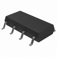
S-24CS01AFJ-TB-G Seiko Instruments, S-24CS01AFJ-TB-G Datasheet - Page 12

S-24CS01AFJ-TB-G
Manufacturer Part Number
S-24CS01AFJ-TB-G
Description
IC EEPROM 1KBIT 400KHZ 8SOP
Manufacturer
Seiko Instruments
Datasheet
1.S-24CS01AFT-TB-G.pdf
(47 pages)
Specifications of S-24CS01AFJ-TB-G
Format - Memory
EEPROMs - Serial
Memory Type
EEPROM
Memory Size
1K (128 x 8)
Speed
400kHz
Interface
I²C, 2-Wire Serial
Voltage - Supply
1.8 V ~ 5.5 V
Operating Temperature
-40°C ~ 85°C
Package / Case
8-SOP
Lead Free Status / RoHS Status
Lead free / RoHS Compliant
Available stocks
Company
Part Number
Manufacturer
Quantity
Price
Company:
Part Number:
S-24CS01AFJ-TB-G
Manufacturer:
SEIKO
Quantity:
576
12
2-WIRE CMOS SERIAL E
S-24CS01A/02A/04A/08A
5. Device Addressing
To start communication, the master device on the system generates a start condition to the bus line. Next,
the master device sends 7-bit device address and a 1-bit read / write instruction code on to the SDA bus.
The 4 most significant bits of the device address are called the "Device Code", and are fixed to "1010".
In S-24CS01A/02A, successive 3 bits are called the “Slave Address”. These 3 bits are used to identify a
device on the system bus and are compared with the predetermined value which is defined by the address
input pins (A0, A1 and A2). When the comparison result matches, the slave device responds with an
acknowledge during the 9th clock cycle.
In S-24CS04A, successive 2 bits are called the "Slave Address". These 2 bits are used to identify a device
on the system bus and are compared with the predetermined value which is defined by the address input
pins (A1 and A2). When the comparison result matches, the slave device responds with an acknowledge
during the 9th clock cycle.
The successive 1 bit (P0) is used to define a page address and choose the two 256-byte memory blocks
(Address 000h to 0FFh and 100h to 1FFh).
In S-24CS08A, successive 1 bit is called the “Slave Addrdess”. This 1 bit is used to identify a device on the
system bus and is compared with the predetermined value which is defined by the address input pin (A2).
When the comparison result matches, the slave device responds with an acknowledge during the 9th
clocks cycle.
The successive 2 bits (P1 and P0) are used to define a page address and choose the four 256-byte
memory blocks (Address 000h to 0FFh, 100h to 1FFh, 200h to 2FFh and 300h to 3FFh).
S-24CS01A/02A
S-24CS04A
S-24CS08A
2
PROM
MSB
MSB
1
1
1
Figure 12 Device Address
Device Code
Device Code
Seiko Instruments Inc.
0
0
0
1
1
1
0
0
0
A2
A2
A2
Slave Address
Slave / Page
Address
A1
A1
P1
A0
P0
P0
R/W
R/W
R/W
LSB
LSB
Rev.4.5
_00


