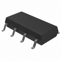
S-24CS01AFJ-TB-G Seiko Instruments, S-24CS01AFJ-TB-G Datasheet - Page 9

S-24CS01AFJ-TB-G
Manufacturer Part Number
S-24CS01AFJ-TB-G
Description
IC EEPROM 1KBIT 400KHZ 8SOP
Manufacturer
Seiko Instruments
Datasheet
1.S-24CS01AFT-TB-G.pdf
(47 pages)
Specifications of S-24CS01AFJ-TB-G
Format - Memory
EEPROMs - Serial
Memory Type
EEPROM
Memory Size
1K (128 x 8)
Speed
400kHz
Interface
I²C, 2-Wire Serial
Voltage - Supply
1.8 V ~ 5.5 V
Operating Temperature
-40°C ~ 85°C
Package / Case
8-SOP
Lead Free Status / RoHS Status
Lead free / RoHS Compliant
Available stocks
Company
Part Number
Manufacturer
Quantity
Price
Company:
Part Number:
S-24CS01AFJ-TB-G
Manufacturer:
SEIKO
Quantity:
576
Rev.4.5
1. Address Input Pins (A0, A1 and A2)
2. SDA (Serial Data Input / Output) Pin
3. SCL (Serial Clock Input) Pin
4. WP Pin
Pin Functions
The slave address is assigned by connecting pins A0, A1 and A2 to the GND or to the V
One of the eight different slave address can be assigned to the S-24CS01A/02A by the combination of
pins A0, A1 and A2.
The slave address is assigned by connecting pins A1 and A2 to the GND or to the V
the four different slave address can be assigned to the S-24CS04A by the combination of pins A1 and A2.
The slave address is assigned by connecting the A2 pin to the GND or to the V
different slave address can be assigned to the S-24CS08A by A2 pin.
The given slave address, which is compared with the slave address transmitted from the master device, is
used to select the one among the multiple devices connected to the bus. The address input pin should be
connected to the GND or to the V
The SDA pin is used for bi-directional transmission of serial data. It consists of a signal input pin and an
Nch open-drain output pin.
The SDA line is usually pulled up to the V
devices.
The SCL pin is used for serial clock input. Since signals are processed at the rising or falling edge of the
SCL clock input signal, attention should be paid to the rising time and falling time to conform to the
specifications.
The write protection is enabled by connecting the WP pin to the V
protection, connect the pin to the GND.
_00
CC
.
Seiko Instruments Inc.
CC
, and OR-wired with other open-drain or open-collector output
2-WIRE CMOS SERIAL E
CC
. When there is no need for write
S-24CS01A/02A/04A/08A
CC
CC
respectively. The two
respectively. One of
CC
respectively.
2
PROM
9


