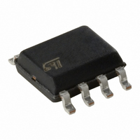
M25P10-AVMN6TP NUMONYX, M25P10-AVMN6TP Datasheet - Page 6

M25P10-AVMN6TP
Manufacturer Part Number
M25P10-AVMN6TP
Description
IC FLASH 1MBIT 50MHZ 8SOIC
Manufacturer
NUMONYX
Series
Forté™r
Datasheet
1.M25P10-AVMP6TG.pdf
(51 pages)
Specifications of M25P10-AVMN6TP
Format - Memory
FLASH
Memory Type
FLASH
Memory Size
1M (128K x 8)
Speed
50MHz
Interface
SPI, 3-Wire Serial
Voltage - Supply
2.3 V ~ 3.6 V
Operating Temperature
-40°C ~ 85°C
Package / Case
8-SOIC (3.9mm Width)
Package
8SO N
Cell Type
NOR
Density
1 Mb
Architecture
Sectored
Block Organization
Symmetrical
Typical Operating Supply Voltage
3.3 V
Sector Size
256Byte x 512
Timing Type
Synchronous
Interface Type
Serial-SPI
Lead Free Status / RoHS Status
Lead free / RoHS Compliant
Other names
M25P10-AVMN6TPTR
Available stocks
Company
Part Number
Manufacturer
Quantity
Price
Company:
Part Number:
M25P10-AVMN6TP
Manufacturer:
MICRON
Quantity:
11 200
Company:
Part Number:
M25P10-AVMN6TP
Manufacturer:
Numonyx
Quantity:
47 500
Company:
Part Number:
M25P10-AVMN6TP
Manufacturer:
ST
Quantity:
144
Company:
Part Number:
M25P10-AVMN6TP
Manufacturer:
MICRON85
Quantity:
4 940
Part Number:
M25P10-AVMN6TP
Manufacturer:
ST
Quantity:
20 000
1
6/51
Description
The M25P10-A is a 1 Mbit (128 Kbit x 8) serial Flash memory, with advanced write
protection mechanisms, accessed by a high speed SPI-compatible bus.
The memory can be programmed 1 to 256 bytes at a time, using the Page Program
instruction.
The memory is organized as 4 sectors, each containing 128 pages. Each page is 256 bytes
wide. Thus, the whole memory can be viewed as consisting of 512 pages, or 131,072 bytes.
The whole memory can be erased using the Bulk Erase instruction, or a sector at a time,
using the Sector Erase instruction.
Figure 1.
Table 1.
C
D
Q
S
W
HOLD
V
V
CC
SS
Signal name
Logic diagram
Signal names
HOLD
W
D
C
S
Serial Clock
Serial Data input
Serial Data output
Chip Select
Write Protect
Hold
Supply voltage
Ground
V CC
V SS
Function
Logic_Diagram_M25P
Q
Input
Input
Output
Input
Input
Input
Direction


