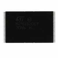
M29W320ET70N6E NUMONYX, M29W320ET70N6E Datasheet - Page 18

M29W320ET70N6E
Manufacturer Part Number
M29W320ET70N6E
Description
IC FLASH 32MBIT 70NS 48TSOP
Manufacturer
NUMONYX
Series
Axcell™r
Specifications of M29W320ET70N6E
Format - Memory
FLASH
Memory Type
FLASH - Nor
Memory Size
32M (4Mx8, 2Mx16)
Speed
70ns
Interface
Parallel
Voltage - Supply
2.7 V ~ 3.6 V
Operating Temperature
-40°C ~ 85°C
Package / Case
48-TSOP
Supply Voltage Range
2.7V To 3.6V
Memory Case Style
TSOP
No. Of Pins
48
Access Time
70ns
Base Number
29
Ic Generic Number
29W320
Memory Configuration
4M X 8, 2M X 16
Interface Type
CFI, Parallel
Rohs Compliant
Yes
Lead Free Status / RoHS Status
Lead free / RoHS Compliant
Other names
497-3608
497-3608
497-3608
Available stocks
Company
Part Number
Manufacturer
Quantity
Price
Company:
Part Number:
M29W320ET70N6E
Manufacturer:
MICRON
Quantity:
15 600
Company:
Part Number:
M29W320ET70N6E
Manufacturer:
Numonyx
Quantity:
23 040
Part Number:
M29W320ET70N6E
Manufacturer:
ST
Quantity:
20 000
3.5
3.6
3.6.1
3.6.2
18/65
Automatic Standby
If CMOS levels (V
more the memory enters Automatic Standby where the internal Supply current is reduced to
the Standby Supply current, I
operation is in progress.
Special bus operations
Additional bus operations can be performed to read the Electronic signature and also to
apply and remove Block Protection. These bus operations are intended for use by
programming equipment and are not usually used in applications. They require V
applied to some pins.
Electronic signature
The memory has two codes, the manufacturer code and the device code, that can be read
to identify the memory. These codes can be read by applying the signals listed in
and
Block Protect and Chip Unprotect
Groups of blocks can be protected against accidental Program or Erase. The Protection
groups are shown in
Addresses. The whole chip can be unprotected to allow the data inside the blocks to be
changed.
The V
V
protected regardless of the Block Protection Status or the Reset/Block Temporary
Unprotect pin status.
Block Protect and Chip Unprotect operations are described in
PP
/Write Protect is at V
Table
PP
/Write Protect pin can be used to protect the two outermost boot blocks. When
3, Bus operations.
CC
Appendix A: Block
± 0.2V) are used to drive the bus and the bus is inactive for 300ns or
IL
the two outermost boot blocks are protected and remain
CC2
. The Data Inputs/Outputs will still output data if a Bus Read
Addresses,
Table 21
and
Appendix D: Block
Table
22, Block
Protection.
ID
Table 2
to be


