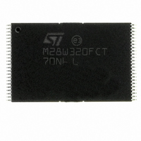
M28W320FCT70N6E NUMONYX, M28W320FCT70N6E Datasheet - Page 52

M28W320FCT70N6E
Manufacturer Part Number
M28W320FCT70N6E
Description
IC FLASH 32MBIT 70NS 48TSOP
Manufacturer
NUMONYX
Datasheet
1.M28W320FCB70ZB6F.pdf
(69 pages)
Specifications of M28W320FCT70N6E
Format - Memory
FLASH
Memory Type
FLASH - Nor
Memory Size
32M (2M x 16)
Speed
70ns
Interface
Parallel
Voltage - Supply
2.7 V ~ 3.6 V
Operating Temperature
-40°C ~ 85°C
Package / Case
48-TSOP
Memory Configuration
2M X 16
Ic Interface Type
Parallel
Access Time
70ns
Supply Voltage Range
2.7V To 3.6V
Memory Case Style
TSOP
No. Of Pins
48
Lead Free Status / RoHS Status
Lead free / RoHS Compliant
Available stocks
Company
Part Number
Manufacturer
Quantity
Price
Company:
Part Number:
M28W320FCT70N6E
Manufacturer:
MICRON
Quantity:
3 000
Company:
Part Number:
M28W320FCT70N6E
Manufacturer:
Numonyx
Quantity:
9 792
Part Number:
M28W320FCT70N6E
Manufacturer:
ST
Quantity:
20 000
Table 27.
1. Query data are always presented on the lowest order data outputs (DQ7-DQ0) only. DQ8-DQ15 are ‘0’.
Table 28.
52/69
Offset
Offset
1Ah
17h
18h
19h
1Ch
1Dh
1Bh
1Eh
1Fh
20h
21h
22h
23h
24h
25h
26h
0000h
0000h
0000h
0000h
Data
CFI Query Identification String
CFI Query System Interface Information
00B4h
00C6h
000Ah
0027h
0036h
0004h
0004h
0000h
0005h
0005h
0003h
0000h
Data
Alternate Vendor Command Set and Control Interface ID Code second
vendor - specified algorithm supported (0000h means none exists)
Address for Alternate Algorithm extended Query table
(0000h means none exists)
V
bit 7 to 4BCD value in volts
bit 3 to 0BCD value in 100 mV
V
bit 7 to 4BCD value in volts
bit 3 to 0BCD value in 100 mV
V
bit 7 to 4HEX value in volts
bit 3 to 0BCD value in 100 mV
V
bit 7 to 4HEX value in volts
bit 3 to 0BCD value in 100 mV
Typical time-out per single word program = 2
Typical time-out for Double/ Quadruple Word Program = 2
Typical time-out per individual block erase = 2
Typical time-out for full chip erase = 2
Maximum time-out for word program = 2
Maximum time-out for Double/ Quadruple Word Program = 2
Maximum time-out per individual block erase = 2
Maximum time-out for chip erase = 2
DD
DD
PP
PP
[Programming] Supply Minimum Program/Erase voltage
[Programming] Supply Maximum Program/Erase voltage
Logic Supply Minimum Program/Erase or Write voltage
Logic Supply Maximum Program/Erase or Write voltage
(1)
Description
(continued)
Description
n
n
times typical
ms
n
times typical
n
n
μs
ms
n
times typical
n
μs
n
times typical
Value
NA
NA
512μs
512μs
Value
12.6V
11.4V
16μs
16μs
2.7V
3.6V
NA
NA
1s
8s


