CY14E256LA-SZ25XI Cypress Semiconductor Corp, CY14E256LA-SZ25XI Datasheet
CY14E256LA-SZ25XI
Specifications of CY14E256LA-SZ25XI
Available stocks


Related parts for CY14E256LA-SZ25XI


CY14E256LA-SZ25XI Summary of contents
Page 1
... Document Number: 001-54952 Rev. *D 256 Kbit (32K x 8) nvSRAM Functional Description The Cypress CY14E256LA is a fast static RAM, with a nonvol- atile element in each memory cell. The memory is organized as 32K bytes of 8 bits each. The embedded nonvolatile elements incorporate QuantumTrap technology, producing the world’s most reliable nonvolatile memory ...
Page 2
... SRAM Write Cycle..................................................... 10 AutoStore/Power Up RECALL ....................................... 12 Software Controlled STORE/RECALL Cycle................ 13 Hardware STORE Cycle ................................................. 14 Truth Table For SRAM Operations................................ 15 Part Numbering Nomenclature...................................... 15 Ordering Information...................................................... 16 Package Diagram............................................................ 16 Document History Page ................................................. 18 Sales, Solutions, and Legal Information ...................... 18 Worldwide Sales and Design Support....................... 18 Products .................................................................... 18 PSoC Solutions ......................................................... 18 CY14E256LA Page [+] Feedback ...
Page 3
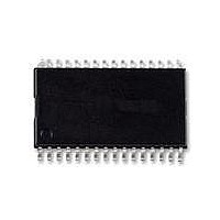
... Address expansion for 4 Mbit. NC pin not connected to die. 4. Address expansion for 8 Mbit. NC pin not connected to die. 5. Address expansion for 16 Mbit. NC pin not connected to die. Document Number: 001-54952 Rev. *D [4] [3] [2] [1] [ Description CY14E256LA 32 - SOIC (x8) Top View (not to scale) ) with standard output high HHHD Page [+] Feedback ...
Page 4
... HSB goes LOW are inhibited until HSB returns HIGH. In case the write latch is not set, HSB is not driven LOW by the CY14E256LA. But any SRAM read and write cycles are inhibited until HSB is returned HIGH by MPU or other external source. ...
Page 5
... L H Notes 6. While there are 15 address lines on the CY14E256LA, only the lower 14 are used to control software modes. 7. The six consecutive address locations must be in the order listed. WE must be HIGH during all six cycles to enable a nonvolatile cycle. Document Number: 001-54952 Rev Read Address 0x0E38 Valid READ 2 ...
Page 6
... Output Data Output Data Output Data Output Data [7] Output Data Active I CC2 Output Data Output Data Output Data Output Data Output High Z [7] Output Data Active Output Data Output Data Output Data Output Data Output High the CY14E256LA write mode Page [+] Feedback ...
Page 7
... V value to make sure there is extra CAP store charge and store time should discuss their V selection with Cypress to understand any impact on the V voltage level at the end period. RECALL CY14E256LA value because CAP charge and CAP value. Customers CAP size ...
Page 8
... Max, V < V < Max, V < V < Max, V < V < > OUT – pin and Rated CAP SS CY14E256LA + 2. 25°C) ....................................................1.0W Ambient Temperature V CC –40°C to +85°C 4.5V to 5.5V [8] Min Typ Max 4.5 5.0 5 STORE 5 –1 +1 –100 + < V – ...
Page 9
... MHz (Typ Test Conditions Test conditions follow standard test methods and procedures for measuring thermal impedance, in accordance with EIA/JESD51. Figure 3. AC Test Loads 5.0V OUTPUT 512Ω CY14E256LA Min Unit 20 Years 1,000 K Max Unit 44-TSOP II 32-SOIC Unit °C/W 41.74 41.55 ° ...
Page 10
... Measured ±200 mV from steady state output voltage. 14 low when CE goes low, the outputs remain in the high impedance state. 15. HSB must remain HIGH during READ and WRITE cycles. Document Number: 001-54952 Rev Description Min [11, 12, 15 Address Valid t AA Output Data Valid t OHA CY14E256LA 45 ns Unit Max Min Max ...
Page 11
... Document Number: 001-54952 Rev. *D Address Valid ACE LZCE t DOE t LZOE Output Data Valid t PU Active [14, 15, 16 Address Valid t SCE PWE Input Data Valid t t LZWE HZWE High Impedance [14, 15, 16 Address Valid SCE t PWE Input Data Valid High Impedance CY14E256LA [11, 15] t HZCE t HZOE Page [+] Feedback ...
Page 12
... Document Number: 001-54952 Rev. *D Description Figure 8. AutoStore or Power Up RECALL 18 t Note STORE t HHHD t LZHSB t DELAY t HRECALL Read & Write BROWN POWER-UP OUT RECALL AutoStore SWITCH. is below V CC SWITCH. CY14E256LA CY14E256LA Min Max 4.4 150 1.9 5 500 [20 Note STORE t 21 HHHD Note t DELAY t LZHSB t HRECALL Read & ...
Page 13
... RC RC Address # HZCE t DELAY Note Figure 10. AutoStore Enable / Disable Cycle t RC Address # HZCE Note Table 2 on page 5. WE must be HIGH during all six consecutive cycles. time. DELAY CY14E256LA Unit Max Min Max 200 200 [23 HHHD t LZHSB High Impedance t /t STORE RECALL ...
Page 14
... HSB pin is driven high to V 100kOhm resistor, HSB driver is disabled SRAM is disabled as long as HSB (IN) is driven low DHSB DHSB [25, 26] Figure 12. Soft Sequence Processing t Soft Sequence SS Command Address #6 Address # CY14E256LA CY14E256LA Unit Min Max μs 100 t HHHD t LZHSB only by Internal Address #6 ...
Page 15
... Document Number: 001-54952 Rev. *D Inputs/Outputs Deselect/Power Down –DQ ); Read 0 7 Output Disabled –DQ ); Write 0 7 Option Tape & Reel Blank - Std. Temperature Industrial (- Package TSOP SOIC Data Bus CY14E256LA Mode Power Standby Active Active Active o C) Speed Density: 256 - 256 Kb Page [+] Feedback ...
Page 16
... Ordering Information Speed Ordering Code (ns) 25 CY14E256LA-SZ25XIT CY14E256LA-SZ25XI 45 CY14E256LA-SZ45XIT CY14E256LA-SZ45XI All the above parts are Pb-free. Package Diagram Document Number: 001-54952 Rev. *D Package Package Type Diagram 51-85127 32-pin SOIC Figure 13. 44-Pin TSOP II (51-85087) CY14E256LA Operating Range Industrial 51-85087 *C Page [+] Feedback ...
Page 17
... Figure 14. 32-Pin SOIC (51-85127) PIN DIMENSIONS IN INCHES[MM] 0.292[7.416] 0.299[7.594] REFERENCE JEDEC MO-119 0.405[10.287] 0.419[10.642] 32 SEATING PLANE 0.090[2.286] 0.100[2.540] 0.004[0.101] 0.026[0.660] 0.032[0.812] 0.004[0.101] 0.0100[0.254] CY14E256LA MIN. MAX. PART # S32.3 STANDARD PKG. SZ32.3 LEAD FREE PKG. 0.006[0.152] 0.021[0.533] 0.012[0.304] 0.041[1.041] 51-85127 *B Page [+] Feedback ...
Page 18
... Document History Page Document Title: CY14E256LA 256 Kbit (32K x 8) nvSRAM Document Number: 001-54952 Orig. of Submission Rev. ECN No. Change ** 2748216 GVCH/PYRS 08/04/09 *A 2772059 GVCH 09/30/09 *B 2829117 GVCH 12/16/09 *C 2891356 GVCH 03/12/10 *D 2922858 GVCH 04/26/10 Sales, Solutions, and Legal Information Worldwide Sales and Design Support Cypress maintains a worldwide network of offices, solution centers, manufacturer’ ...