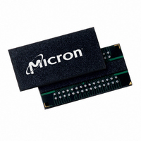
MT47H128M4B6-3:D TR Micron Technology Inc, MT47H128M4B6-3:D TR Datasheet - Page 113

MT47H128M4B6-3:D TR
Manufacturer Part Number
MT47H128M4B6-3:D TR
Description
IC DDR2 SDRAM 512MBIT 3NS 60FBGA
Manufacturer
Micron Technology Inc
Datasheet
1.MT47H128M4BT-37EA_TR.pdf
(129 pages)
Specifications of MT47H128M4B6-3:D TR
Format - Memory
RAM
Memory Type
DDR2 SDRAM
Memory Size
512M (128Mx4)
Speed
3ns
Interface
Parallel
Voltage - Supply
1.7 V ~ 1.9 V
Operating Temperature
0°C ~ 85°C
Package / Case
60-FBGA
Lead Free Status / RoHS Status
Lead free / RoHS Compliant
Other names
557-1291-2
MT47H128M4B6-3:D TR
MT47H128M4B6-3:D TR
- Current page: 113 of 129
- Download datasheet (10Mb)
Power-Down Mode
PDF: 09005aef82f1e6e2
512MbDDR2.pdf - Rev. O 7/09 EN
DDR2 SDRAM supports multiple power-down modes that allow significant power sav-
ings over normal operating modes. CKE is used to enter and exit different power-down
modes. Power-down entry and exit timings are shown in Figure 68 (page 114). Detailed
power-down entry conditions are shown in Figure 69 (page 116)–Figure 76 (page 119).
Table 43 (page 115) is the CKE Truth Table.
DDR2 SDRAM requires CKE to be registered HIGH (active) at all times that an access is
in progress—from the issuing of a READ or WRITE command until completion of the
burst. Thus, a clock suspend is not supported. For READs, a burst completion is defined
when the read postamble is satisfied; for WRITEs, a burst completion is defined when
the write postamble and
READ command) are satisfied, as shown in Figure 71 (page 117) and Figure 72
(page 117) on Figure 72 (page 117). The number of clock cycles required to meet
is either two or
Power-down mode (see Figure 68 (page 114)) is entered when CKE is registered low
coincident with an NOP or DESELECT command. CKE is not allowed to go LOW during
a mode register or extended mode register command time, or while a READ or WRITE
operation is in progress. If power-down occurs when all banks are idle, this mode is
referred to as precharge power-down. If power-down occurs when there is a row active
in any bank, this mode is referred to as active power-down. Entering power-down deac-
tivates the input and output buffers, excluding CK, CK#, ODT, and CKE. For maximum
power savings, the DLL is frozen during precharge power-down. Exiting active power-
down requires the device to be at the same voltage and frequency as when it entered
power-down. Exiting precharge power-down requires the device to be at the same volt-
age as when it entered power-down; however, the clock frequency is allowed to change
(see Precharge Power-Down Clock Frequency Change (page 120)).
The maximum duration for either active or precharge power-down is limited by the re-
fresh requirements of the device
entry and exit is limited by the
tained while in power-down mode: CKE LOW, a stable clock signal, and stable power
supply signals at the inputs of the DDR2 SDRAM. All other input signals are “Don’t
Care” except ODT. Detailed ODT timing diagrams for different power-down modes are
shown in Figure 81 (page 125)–Figure 86 (page 129).
The power-down state is synchronously exited when CKE is registered HIGH (in con-
junction with a NOP or DESELECT command), as shown in Figure 68 (page 114).
t
WTR/
t
CK, whichever is greater.
t
WR (WRITE-to-PRECHARGE command) or
113
t
CKE (MIN) parameter. The following must be main-
t
RFC (MAX). The minimum duration for power-down
Micron Technology, Inc. reserves the right to change products or specifications without notice.
512Mb: x4, x8, x16 DDR2 SDRAM
Power-Down Mode
©2004 Micron Technology, Inc. All rights reserved.
t
WTR (WRITE-to-
t
WTR
Related parts for MT47H128M4B6-3:D TR
Image
Part Number
Description
Manufacturer
Datasheet
Request
R

Part Number:
Description:
IC SDRAM 64MBIT 133MHZ 54TSOP
Manufacturer:
Micron Technology Inc
Datasheet:

Part Number:
Description:
IC SDRAM 64MBIT 5.5NS 86TSOP
Manufacturer:
Micron Technology Inc
Datasheet:

Part Number:
Description:
IC SDRAM 64MBIT 200MHZ 86TSOP
Manufacturer:
Micron Technology Inc
Datasheet:

Part Number:
Description:
IC SDRAM 64MBIT 133MHZ 54TSOP
Manufacturer:
Micron Technology Inc
Datasheet:

Part Number:
Description:
IC SDRAM 128MBIT 133MHZ 54TSOP
Manufacturer:
Micron Technology Inc
Datasheet:

Part Number:
Description:
IC SDRAM 256MBIT 133MHZ 90VFBGA
Manufacturer:
Micron Technology Inc
Datasheet:

Part Number:
Description:
IC SDRAM 128MBIT 133MHZ 54TSOP
Manufacturer:
Micron Technology Inc
Datasheet:

Part Number:
Description:
IC SDRAM 256MBIT 133MHZ 54TSOP
Manufacturer:
Micron Technology Inc
Datasheet:

Part Number:
Description:
IC DDR SDRAM 512MBIT 6NS 66TSOP
Manufacturer:
Micron Technology Inc
Datasheet:

Part Number:
Description:
IC SDRAM 128MBIT 167MHZ 86TSOP
Manufacturer:
Micron Technology Inc
Datasheet:

Part Number:
Description:
IC SDRAM 128MBIT 143MHZ 86TSOP
Manufacturer:
Micron Technology Inc
Datasheet:

Part Number:
Description:
SDRAM 256M-BIT 1.8V 54-PIN VFBGA
Manufacturer:
Micron Technology Inc
Datasheet:

Part Number:
Description:
IC SDRAM 128MBIT 143MHZ 86TSOP
Manufacturer:
Micron Technology Inc
Datasheet:

Part Number:
Description:
IC SDRAM 128MBIT 125MHZ 54VFBGA
Manufacturer:
Micron Technology Inc
Datasheet:

Part Number:
Description:
IC SDRAM 128MBIT 125MHZ 54VFBGA
Manufacturer:
Micron Technology Inc
Datasheet:


