DS1251YP-70IND+ Maxim Integrated Products, DS1251YP-70IND+ Datasheet - Page 3
DS1251YP-70IND+
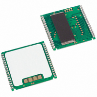
Manufacturer Part Number
DS1251YP-70IND+
Description
IC NVSRAM 4MBIT 70NS 34PCM
Manufacturer
Maxim Integrated Products
Datasheet
1.DS1251Y-70.pdf
(21 pages)
Specifications of DS1251YP-70IND+
Format - Memory
RAM
Memory Type
NVSRAM (Non-Volatile SRAM)
Memory Size
4M (512K x 8)
Speed
70ns
Interface
Parallel
Voltage - Supply
4.5 V ~ 5.5 V
Operating Temperature
-40°C ~ 85°C
Package / Case
34-PowerCap™ Module
Lead Free Status / RoHS Status
Lead free / RoHS Compliant


PIN DESCRIPTION (continued)
DESCRIPTION
The DS1251 4096k NV SRAM with Phantom Clock is a fully static nonvolatile RAM (organized as 512k
words by 8 bits) with a built-in real-time clock. The DS1251Y has a self-contained lithium energy source
and control circuitry, which constantly monitors V
condition occurs, the lithium energy source is automatically switched on and write protection is
unconditionally enabled to prevent garbled data in both the memory and real-time clock.
The phantom clock provides timekeeping information including hundredths of seconds, seconds, minutes,
hours, days, dates, months, and years. The date at the end of the month is automatically adjusted for
months with fewer than 31 days, including correction for leap years. The phantom clock operates in either
24-hour or 12-hour format with an AM/PM indicator.
PACKAGES
The DS1251 is available in two packages: 32-pin DIP and 34-pin PowerCap module. The 32-pin DIP
style module integrates the crystal, lithium energy source, and silicon in one package. The 34-pin
PowerCap module board is designed with contacts for connection to a separate PowerCap (DS9034PCX)
that contains the crystal and battery. This design allows the PowerCap to be mounted on top of the
DS1251P after the completion of the surface mount process. Mounting the PowerCap after the surface
mount process prevents damage to the crystal and battery because of the high temperatures required for
solder reflow. The PowerCap is keyed to prevent reverse insertion. The PowerCap Module Board and
PowerCap are ordered separately and shipped in separate containers.
RAM READ MODE
The DS1251 executes a read cycle whenever
active (low). The unique address specified by the 19 address inputs (A0–A18) defines which of the 512k
bytes of data is to be accessed. Valid data will be available to the eight data-output drivers within t
(access time) after the last address input signal is stable, providing that
times and states are also satisfied. If
measured from the later occurring signal (
t
RAM WRITE MODE
The DS1251 is in the write mode whenever the
address inputs are stable. The latter occurring falling edge of
write cycle. The write cycle is terminated by the earlier rising edge of
OE
EDIP
22
24
29
32
16
—
for
OE
PIN
PowerCap
, rather than address access.
17
8
7
6
5
4
NAME
GND
N.C.
V
WE
CE
OE
CC
Active-Low Chip-Enable Input
Active-Low Output-Enable Input
Active-Low Write-Enable Input
Power-Supply Input
No Connection
Ground
OE
and
C E
WE
CE
or
3 of 21
(write enable) is inactive (high) and
access times are not satisfied, then data access must be
WE
O
E
CC
) and the limiting parameter is either t
and
for an out-of-tolerance condition. When such a
CE
FUNCTION
CE
signals are in the active (low) state after
or
CE
WE
CE
or
and
will determine the start of the
WE
OE
. All address inputs must
(output enable) access
CE
(chip enable) is
CO
f
or
CE
ACC
or
Related parts for DS1251YP-70IND+
Image
Part Number
Description
Manufacturer
Datasheet
Request
R

Part Number:
Description:
IC NVSRAM 4MBIT 70NS 34PCM
Manufacturer:
Maxim Integrated Products
Datasheet:
Part Number:
Description:
IC NVSRAM 4MBIT 70NS 34PCM
Manufacturer:
Maxim Integrated Products
Datasheet:

Part Number:
Description:
Real Time Clock
Manufacturer:
Maxim Integrated Products
Datasheet:

Part Number:
Description:
The DS1251 4096K NV SRAM with Phantom Clock is a fully static nonvolatile RAM (organized as 512K words by 8 bits) with a built-in real-time clock
Manufacturer:
Maxim
Datasheet:
Part Number:
Description:
Real Time Clock 4096K NV SRAM w/Phantom Clock
Manufacturer:
Maxim Integrated
Datasheet:
Part Number:
Description:
Real Time Clock 4096K NV SRAM w/Phantom Clock
Manufacturer:
Maxim Integrated
Datasheet:
Part Number:
Description:
MAX7528KCWPMaxim Integrated Products [CMOS Dual 8-Bit Buffered Multiplying DACs]
Manufacturer:
Maxim Integrated Products
Datasheet:
Part Number:
Description:
Single +5V, fully integrated, 1.25Gbps laser diode driver.
Manufacturer:
Maxim Integrated Products
Datasheet:
Part Number:
Description:
Single +5V, fully integrated, 155Mbps laser diode driver.
Manufacturer:
Maxim Integrated Products
Datasheet:
Part Number:
Description:
VRD11/VRD10, K8 Rev F 2/3/4-Phase PWM Controllers with Integrated Dual MOSFET Drivers
Manufacturer:
Maxim Integrated Products
Datasheet:
Part Number:
Description:
Highly Integrated Level 2 SMBus Battery Chargers
Manufacturer:
Maxim Integrated Products
Datasheet:
Part Number:
Description:
Current Monitor and Accumulator with Integrated Sense Resistor; ; Temperature Range: -40°C to +85°C
Manufacturer:
Maxim Integrated Products
Part Number:
Description:
TSSOP 14/A°/RS-485 Transceivers with Integrated 100O/120O Termination Resis
Manufacturer:
Maxim Integrated Products
Part Number:
Description:
TSSOP 14/A°/RS-485 Transceivers with Integrated 100O/120O Termination Resis
Manufacturer:
Maxim Integrated Products
Part Number:
Description:
QFN 16/A°/AC-DC and DC-DC Peak-Current-Mode Converters with Integrated Step
Manufacturer:
Maxim Integrated Products