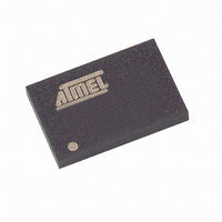
AT45DB081B-CC Atmel, AT45DB081B-CC Datasheet - Page 7

AT45DB081B-CC
Manufacturer Part Number
AT45DB081B-CC
Description
IC FLASH 8MBIT 20MHZ 14CBGA
Manufacturer
Atmel
Datasheet
1.AT45DB081B-CC.pdf
(33 pages)
Specifications of AT45DB081B-CC
Format - Memory
FLASH
Memory Type
DataFLASH
Memory Size
8M (4096 pages x 264 bytes)
Speed
20MHz
Interface
SPI, 3-Wire Serial
Voltage - Supply
2.7 V ~ 3.6 V
Operating Temperature
0°C ~ 70°C
Package / Case
14-CBGA
Lead Free Status / RoHS Status
Contains lead / RoHS non-compliant
Available stocks
Company
Part Number
Manufacturer
Quantity
Price
Company:
Part Number:
AT45DB081B-CC
Manufacturer:
ATMEL
Quantity:
1 831
Additional Commands
2225J–DFLSH–2/08
should take place in a maximum of time t
cate that the part is busy.
MAIN MEMORY PAGE TO BUFFER TRANSFER: A page of data can be transferred
from the main memory to either buffer 1 or buffer 2. To start the operation, an 8-bit
opcode, 53H for buffer 1 and 55H for buffer 2, must be followed by the three reserved
bits, 12 address bits (PA11 - PA0) which specify the page in main memory that is to be
transferred, and nine don’t care bits. The CS pin must be low while toggling the SCK pin
to load the opcode, the address bits, and the don’t care bits from the SI pin. The transfer
of the page of data from the main memory to the buffer will begin when the CS pin tran-
sitions from a low to a high state. During the transfer of a page of data (t
register can be read to determine whether the transfer has been completed or not.
MAIN MEMORY PAGE TO BUFFER COMPARE: A page of data in main memory can
be compared to the data in buffer 1 or buffer 2. To initiate the operation, an 8-bit opcode,
60H for buffer 1 and 61H for buffer 2, must be followed by 24 address bits consisting of
the three reserved bits, 12 address bits (PA11 - PA0) which specify the page in the main
memory that is to be compared to the buffer, and nine don’t care bits. The CS pin must
be low while toggling the SCK pin to load the opcode, the address bits, and the don’t
care bits from the SI pin. On the low-to-high transition of the CS pin, the 264 bytes in the
selected main memory page will be compared with the 264 bytes in buffer 1 or buffer 2.
During this time (t
tion of the compare operation, bit 6 of the status register is updated with the result of the
compare.
AUTO PAGE REWRITE: This mode is only needed if multiple bytes within a page or
multiple pages of data are modified in a random fashion. This mode is a combination of
two operations: Main Memory Page to Buffer Transfer and Buffer to Main Memory Page
Program with Built-in Erase. A page of data is first transferred from the main memory to
buffer 1 or buffer 2, and then the same data (from buffer 1 or buffer 2) is programmed
back into its original page of main memory. To start the rewrite operation, an 8-bit
opcode, 58H for buffer 1 or 59H for buffer 2, must be followed by the three reserved bits,
12 address bits (PA11 - PA0) that specify the page in main memory to be rewritten, and
nine additional don’t care bits. When a low-to-high transition occurs on the CS pin, the
part will first transfer data from the page in main memory to a buffer and then program
the data from the buffer back into same page of main memory. The operation is inter-
nally self-timed and should take place in a maximum time of t
status register will indicate that the part is busy.
XFR
), the status register will indicate that the part is busy. On comple-
EP
. During this time, the status register will indi-
AT45DB081B
EP
. During this time, the
XFR
), the status
7


