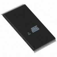
AT49F4096A-90TC Atmel, AT49F4096A-90TC Datasheet - Page 5

AT49F4096A-90TC
Manufacturer Part Number
AT49F4096A-90TC
Description
IC FLASH 4MBIT 90NS 48TSOP
Manufacturer
Atmel
Datasheet
1.AT49F4096A-90RC.pdf
(15 pages)
Specifications of AT49F4096A-90TC
Format - Memory
FLASH
Memory Type
FLASH
Memory Size
4M (512K x 8 or 256K x 16)
Speed
90ns
Interface
Parallel
Voltage - Supply
4.5 V ~ 5.5 V
Operating Temperature
0°C ~ 70°C
Package / Case
48-TSOP
Lead Free Status / RoHS Status
Contains lead / RoHS non-compliant
Available stocks
Company
Part Number
Manufacturer
Quantity
Price
Company:
Part Number:
AT49F4096A-90TC
Manufacturer:
ATM
Quantity:
3 586
Company:
Part Number:
AT49F4096A-90TC
Manufacturer:
ATM
Quantity:
3 586
Company:
Part Number:
AT49F4096A-90TC
Manufacturer:
TOSHIBA
Quantity:
4 130
Part Number:
AT49F4096A-90TC
Manufacturer:
ATMEL/爱特梅尔
Quantity:
20 000
For details, see Operating Modes (for hardware operation)
or Software Product Identification. The manufacturer and
device code is the same for both modes.
DATA POLLING: The AT49F004(T)/4096A(T) features
DATA polling to indicate the end of a program cycle. During
a program cycle an attempted read of the last byte loaded
will result in the complement of the loaded data on I/O7.
Once the program cycle has been completed, true data is
valid on all outputs and the next cycle may begin. During a
chip or sector erase operation, an attempt to read the
device will give a “0” on I/O7. Once the program or erase
cycle has completed, true data will be read from the device.
DATA polling may begin at any time during the program
cycle.
T O G G L E B I T : I n a d d i t i o n t o DATA p o l l i n g t h e
AT49F004(T)/4096A(T) provides another method for deter-
mining the end of a program or erase cycle. During a pro-
gram or erase operation, successive attempts to read data
from the device will result in I/O6 toggling between one and
zero. Once the program cycle has completed, I/O6 will stop
toggling and valid data will be read. Examining the toggle
bit may begin at any time during a program cycle.
READY/BUSY: For the AT49F004(T), pin 12 is an open
drain READY/BUSY output pin which provides another
method of detecting the end of a program or erase opera-
tion. RDY/BUSY is actively pulled low during the internal
program and erase cycles and it is released at the comple-
tion of the cycle. The open drain connection allows for OR-
tying of several devices to the same RDY/BUSY line.
HARDWARE DATA PROTECTION: Hardware features
p r o t e c t a g a i n s t i n a d v e r t e n t p r o g r a m s t o t h e
AT49F004(T)/4096A(T) in the following ways: (a) V
sense: if V
is inhibited. (b) V
the V
10 ms (typical) before programming. (c) Program inhibit:
holding any one of OE low, CE high or WE high inhibits
program cycles. (d) Noise filter: pulses of less than 15 ns
(typical) on the WE or CE inputs will not initiate a program
cycle.
CC
sense level, the device will automatically time out
CC
is below 3.8V (typical), the program function
CC
power on delay: once V
CC
has reached
CC
5


