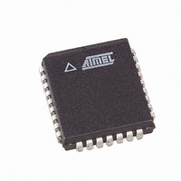
AT45DB011-JI Atmel, AT45DB011-JI Datasheet - Page 3

AT45DB011-JI
Manufacturer Part Number
AT45DB011-JI
Description
IC FLASH 1MBIT 13MHZ 32PLCC
Manufacturer
Atmel
Datasheet
1.AT45DB011-JC.pdf
(20 pages)
Specifications of AT45DB011-JI
Format - Memory
FLASH
Memory Type
DataFLASH
Memory Size
1M (512 pages x 264 bytes)
Speed
13MHz
Interface
SPI, 3-Wire Serial
Voltage - Supply
2.7 V ~ 3.6 V
Operating Temperature
-40°C ~ 85°C
Package / Case
32-PLCC
Lead Free Status / RoHS Status
Contains lead / RoHS non-compliant
Other names
AT45DB011JI
Memory Architecture Diagram
Device Operation
The device operation is controlled by instructions from the
host processor. The list of instructions and their associated
opcodes are contained in Tables 1 and 2. A valid instruc-
tion starts with the falling edge of CS followed by the
appropriate 8-bit opcode and the desired buffer or main
memory address location. While the CS pin is low, toggling
the SCK pin controls the loading of the opcode and the
desired buffer or main memory address location through
the SI (serial input) pin. All instructions, addresses, and
data are transferred with the most significant bit (MSB) first.
Read
By specifying the appropriate opcode, data can be read
from the main memory or from the data buffer.
MAIN MEMORY PAGE READ: A main memory read allows
the user to read data directly from any one of the 512
pages in the main memory, bypassing the data buffer and
leaving the contents of the buffer unchanged. To start a
page read, the 8-bit opcode, 52H, is followed by 24
address bits and 32 don’t care bits. In the AT45DB011, the
first six address bits are reserved for larger density devices
(see Notes on page 9), the next nine address bits (PA8-
PA0) specify the page address, and the next nine address
SECTOR 1 = 65,472 BYTES (62K + 1984)
SECTOR 2 = 67,584 BYTES (64K + 2K)
SECTOR ARCHITECTURE
SECTOR 0 = 2112 BYTES (2K + 64)
SECTOR 0
BLOCK ARCHITECTURE
Block = 2112 bytes
BLOCK 61
BLOCK 62
BLOCK 63
BLOCK 29
BLOCK 30
BLOCK 31
BLOCK 32
BLOCK 33
BLOCK 34
BLOCK 0
BLOCK 1
BLOCK 2
BLOCK 3
(2K + 64)
bits (BA8-BA0) specify the starting byte address within the
page. The 32 don’t care bits which follow the 24 address
bits are sent to initialize the read operation. Following the
32 don’t care bits, additional pulses on SCK result in serial
data being output on the SO (serial output) pin. The CS pin
must remain low during the loading of the opcode, the
address bits, and the reading of data. When the end of a
page in main memory is reached during a main memory
page read, the device will continue reading at the beginning
of the same page. A low-to-high transition on the CS pin
will terminate the read operation and tri-state the SO pin.
BUFFER READ: Data can be read from the data buffer
using an opcode of 54H. To perform a buffer read, the eight
bits of the opcode must be followed by 15 don’t care bits,
nine address bits, and eight don’t care bits. Since the buffer
size is 264-bytes, nine address bits (BFA8-BFA0) are
required to specify the first byte of data to be read from the
buffer. The CS pin must remain low during the loading of
the opcode, the address bits, the don’t care bits, and the
reading of data. When the end of the buffer is reached, the
device will continue reading back at the beginning of the
buffer. A low-to-high transition on the CS pin will terminate
the read operation and tri-state the SO pin.
8 Pages
PAGE ARCHITECTURE
Page = 264 bytes
PAGE 509
PAGE 510
PAGE 511
PAGE 14
PAGE 15
PAGE 16
PAGE 17
PAGE 18
PAGE 0
PAGE 1
PAGE 6
PAGE 7
PAGE 8
PAGE 9
(256 + 8)
3


