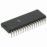
AT49F001N-70PI Atmel, AT49F001N-70PI Datasheet

AT49F001N-70PI
Specifications of AT49F001N-70PI
Related parts for AT49F001N-70PI
AT49F001N-70PI Summary of contents
Page 1
... Output Enable WE Write Enable RESET RESET I/O0 - I/O7 Data Inputs/Outputs NC No Connect DC Don’t Connect PLCC Top View A14 A13 A11 A10 I/ I/O7 Note: *This pin the AT49F001N(T). DIP Top View * RESET 1 32 VCC A16 A15 A12 4 29 A14 A13 A11 A10 ...
Page 2
... When the device is deselected, the CMOS standby current is less than 100 A. For the AT49F001N(T) pin 1 for the DIP and PLCC packages and pin 9 for the TSOP package are don’t connect pins. ...
Page 3
... Boot Block Pro- gramming Lockout Override section). The RESET feature is not available for the AT49F001N(T). ERASURE: Before a byte can be reprogrammed, the main memory block or parameter block which contains the byte must be erased. The erased state of the memory bits is a logical “1”. ...
Page 4
... AT49F001(N)T. Once the feature is enabled, the data in the boot block can no longer be erased or pro- grammed with input voltage levels of 5.5V or less. Data in the main memory block can still be changed through the regular programming method. To activate the lockout feature, a series of six program commands to specific addresses with specific data must be performed ...
Page 5
... When the RESET pin is brought back to TTL levels the boot block programming lockout feature is again active. This feature is not available on the AT49F001N(T). PRODUCT IDENTIFICATION: The product identification mode identifies the device and man- ufacturer as Atmel ...
Page 6
... SA = 18000 to 19FFF for PARAMETER BLOCK 10000 to 17FFF for MAIN MEMORY ARRAY BLOCK 1 This command will erase - PB1, PB2 and MMB1 SA = 00000 to 0FFFF for MAIN MEMORY ARRAY BLOCK 2 Absolute Maximum Ratings* Temperature Under Bias................................ -55°C to +125°C Storage Temperature ..................................... -65°C to +150°C ...
Page 7
... X can Refer to AC Programming Waveforms 12.0V ± 0.5V Manufacturer Code: 1FH, Device Code: 05H - AT49F001(N), 04H - AT49F001(N)T 5. See details under Software Product Identification Entry/Exit. 6. This pin is not available on the AT49F001N(T). DC Characteristics Symbol Parameter I Input Load Current LI I Output Leakage Current LO I ...
Page 8
AC Read Characteristics Symbol Parameter t Address to Output Delay ACC ( Output Delay CE ( Output Delay OE (3)( Output Float DF Output Hold from OE ...
Page 9
Input Test Waveform and Measurement Level Output Load Test Pin Capacitance ( MHz 25°C Symbol Typ OUT Note: 1. This parameter is characterized and is ...
Page 10
AC Byte Load Characteristics Symbol Parameter Address, OE Set-up Time AS OES t Address Hold Time AH t Chip Select Set-up Time CS t Chip Select Hold Time CH t Write Pulse Width (WE or CE) WP ...
Page 11
Program Cycle Characteristics Symbol Parameter t Byte Programming Time BP t Address Set-up Time AS t Address Hold Time AH t Data Set-up Time DS t Data Hold Time DH t Write Pulse Width WP t Write Pulse Width High ...
Page 12
Data Polling Characteristics Symbol Parameter t Data Hold Time Hold Time OEH ( Output Delay OE t Write Recovery Time WR Notes: 1. These parameters are characterized and not 100% tested. 2. See t ...
Page 13
Software Product Identification Entry LOAD DATA AA TO ADDRESS 5555 LOAD DATA 55 TO ADDRESS 2AAA LOAD DATA 90 TO ADDRESS 5555 ENTER PRODUCT IDENTIFICATION (2)(3)(5) MODE Software Product Identification Exit OR LOAD DATA AA TO ADDRESS 5555 LOAD DATA ...
Page 14
AT49F001 Ordering Information I (mA ACC (ns) Active Standby 55 50 0 0 0.1 50 0.3 120 50 0.1 50 0.3 32J 32-lead, Plastic, J-leaded Chip Carrier Package (PLCC) 32P6 ...
Page 15
... AT49F001N-55VC 32V AT49F001N-55JI 32J AT49F001N-55PI 32P6 AT49F001N-55TI 32T AT49F001N-55VI 32V AT49F001N-70JC 32J AT49F001N-70PC 32P6 AT49F001N-70TC 32T AT49F001N-70VC 32V AT49F001N-70JI 32J AT49F001N-70PI 32P6 AT49F001N-70TI 32T AT49F001N-70VI 32V AT49F001N-90JC 32J AT49F001N-90PC 32P6 AT49F001N-90TC 32T AT49F001N-90VC 32V AT49F001N-90JI 32J AT49F001N-90PI 32P6 AT49F001N-90TI 32T AT49F001N-90VI ...
Page 16
AT49F001T Ordering Information I (mA ACC (ns) Active Standby 55 50 0 0 0.1 50 0.3 120 50 0.1 50 0.3 32J 32-lead, Plastic, J-leaded Chip Carrier Package (PLCC) 32P6 ...
Page 17
... AT49F001NT Ordering Information t ACC (ns) I (mA 0 0 0.1 50 0.3 120 50 0.1 50 0.3 32J 32-lead, Plastic, J-leaded Chip Carrier Package (PLCC) 32P6 32-lead, 0.600" Wide, Plastic Dual In-line Package (PDIP) 32T 32-lead, Plastic Thin Small Outline Package (TSOP) 32V 32-lead, Plastic Thin Small Outline Package (VSOP mm) 1008D– ...
Page 18
Packaging Information 32J – PLCC 1.14(0.045) X 45˚ 0.51(0.020)MAX 45˚ MAX (3X) Notes: 1. This package conforms to JEDEC reference MS-016, Variation AE. 2. Dimensions D1 and E1 do not include mold protrusion. Allowable protrusion is .010"(0.254 mm) ...
Page 19
PDIP A SEATING PLANE Note: 1. Dimensions D and E1 do not include mold Flash or Protrusion. Mold Flash or Protrusion shall not exceed 0.25 mm (0.010"). 2325 Orchard Parkway San Jose, CA 95131 R ...
Page 20
TSOP Pin 1 Identifier e E Notes: 1. This package conforms to JEDEC reference MO-142, Variation BD. 2. Dimensions D1 and E do not include mold protrusion. Allowable protrusion 0.15 mm per side and on ...
Page 21
VSOP Pin 1 Identifier e E Notes: 1. This package conforms to JEDEC reference MO-142, Variation BA. 2. Dimensions D1 and E do not include mold protrusion. Allowable protrusion 0.15 mm per side and on ...
Page 22
... No licenses to patents or other intellectual property of Atmel are granted by the Company in connection with the sale of Atmel products, expressly or by implication. Atmel’s products are not authorized for use as critical components in life support devices or systems. ...


